|
Motor de Búsqueda de Datasheet de Componentes Electrónicos |
|
|
Motor de Búsqueda de Datasheet de Componentes Electrónicos |
|
TPS5432 Datasheet(PDF) 10 Page - Texas Instruments |
|
|
|||||||||||||||||||||||||||||
TPS5432 Datasheet(HTML) 10 Page - Texas Instruments |
|
|
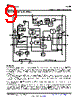
10 / 31 page  TPS5432 SLVSB89A – MARCH 2012 – REVISED OCTOBER 2012 www.ti.com The TPS5432 minimizes excessive output over-voltage transients by taking advantage of the over-voltage comparator. When the regulated output voltage is greater than 107% of the nominal voltage, the over-voltage comparator is activated, and the high side MOSFET is turned off and masked from turning on until the output voltage is lower than 105%. The SS (slow start) pin is used to minimize inrush currents during power up. A small value capacitor should be coupled to the pin for slow start. The SS pin is discharged before the output power up to ensure a repeatable restart after an over-temperature fault, UVLO fault or disabled condition. The use of a frequency fold-back circuit reduces the switching frequency during startup and over current fault conditions to help limit the inductor current. DETAILED DESCRIPTION FIXED FREQUENCY PWM CONTROL The TPS5432 uses a fixed frequency, peak current mode control. The output voltage is compared through external resistors on the VSENSE pin to an internal voltage reference by an error amplifier which drives the COMP pin. An internal oscillator initiates the turn on of the high side power switch. The error amplifier output is compared to the high side power switch current. When the power switch current reaches the COMP voltage level the high side power switch is turned off and the low side power switch is turned on. The COMP pin voltage increases and decreases as the output current increases and decreases. The device implements a current limit by clamping the COMP pin voltage to a maximum level and also implements a minimum clamp for improved transient response performance. SLOPE COMPENSATION AND OUTPUT CURRENT The TPS5432 adds a compensating ramp to the switch current signal. This slope compensation prevents sub- harmonic oscillations as duty cycle increases. The available peak inductor current remains constant over the full duty cycle range. BOOTSTRAP VOLTAGE (BOOT) The TPS5432 has an integrated boot regulator and requires a small ceramic capacitor between the BOOT and PH pin to provide the gate drive voltage for the high side MOSFET. The value of the ceramic capacitor should be 0.1 μF. A ceramic capacitor with an X7R or X5R grade dielectric with a voltage rating of 10 V or higher is recommended because of the stable characteristics over temperature and voltage. The high side MOSFET is turned off using an UVLO circuit, allowing for the low side MOSFET to conduct when the voltage from BOOT to PH drops below 2.1 V. The device may work at 100% duty ratio as long as the BOOT-PH voltage is higher than the BOOT-PH UVLO threshold; but, do not operate the device at 100% duty ratio with no load. See additional information regarding 100% duty ratio in the ENABLE AND UNDERVOLTAGE LOCKOUT section. ERROR AMPLIFIER The TPS5432 has a transconductance amplifier. The error amplifier compares the VSENSE voltage to the lower of the SS pin voltage or the internal 0.808 V voltage reference. The transconductance of the error amplifier is 245 μA/V during normal operation. When the voltage of VSENSE pin is below 0.808 V and the device is regulating using the SS voltage, the gm is 70 μA/V. The frequency compensation components are placed between the COMP pin and ground. VOLTAGE REFERENCE The voltage reference system produces a precise ±3% voltage reference over temperature by scaling the output of a temperature stable bandgap circuit. The bandgap and scaling circuits produce 0.808 V at the non-inverting input of the error amplifier. 10 Submit Documentation Feedback Copyright © 2012, Texas Instruments Incorporated Product Folder Links: TPS5432 |
|
Enlace URL |
| ¿ALLDATASHEET es útil para Ud.? [ DONATE ] |
Todo acerca de Alldatasheet | Publicidad | Contáctenos | Política de Privacidad | Enlace a la hoja de datos | Intercambio de Enlaces | Lista de Fabricantes All Rights Reserved©Alldatasheet.com |
| Russian : Alldatasheetru.com | Korean : Alldatasheet.co.kr | Spanish : Alldatasheet.es | French : Alldatasheet.fr | Italian : Alldatasheetit.com Portuguese : Alldatasheetpt.com | Polish : Alldatasheet.pl | Vietnamese : Alldatasheet.vn Indian : Alldatasheet.in | Mexican : Alldatasheet.com.mx | British : Alldatasheet.co.uk | New Zealand : Alldatasheet.co.nz |
|
Family Site : ic2ic.com |
icmetro.com |
 Mexican ▼
 English
 Chinese
 German
 Japanese
 Russian
 Korean
 Spanish
 French
 Italian
 Portuguese
 Polish
 Vietnamese
 Indian
 Mexican
 British
 New Zealand