|
Motor de Búsqueda de Datasheet de Componentes Electrónicos |
|
|
Motor de Búsqueda de Datasheet de Componentes Electrónicos |
|
9601-00 Datasheet(PDF) 3 Page - Peregrine Semiconductor Corp. |
|
|
|||||||||||||||||||||||||||||
9601-00 Datasheet(HTML) 3 Page - Peregrine Semiconductor Corp. |
|
|
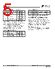
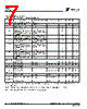
3 / 14 page  Product Specification PE9601 Page 3 of 14 Document No. 70-0025-05 │ www.psemi.com ©2005 Peregrine Semiconductor Corp. All rights reserved. 13 S_WR Serial Input Serial load enable input. While S_WR is “low”, Sdata can be serially clocked. Primary register data are transferred to the secondary register on S_WR or Hop_WR rising edge. D4 Parallel Input Parallel data bus bit4 M4 Direct Input M Counter bit4 14 Sdata Serial Input Binary serial data input. Input data entered MSB first. D5 Parallel Input Parallel data bus bit5. M5 Direct Input M Counter bit5. 15 Sclk Serial Input Serial clock input. Sdata is clocked serially into the 20-bit primary register (E_WR “low”) or the 8-bit enhancement register (E_WR “high”) on the rising edge of Sclk. D6 Parallel Input Parallel data bus bit6. M6 Direct Input M Counter bit6. 16 FSELS Serial Input Selects contents of primary register (FSELS=1) or secondary register (FSELS=0) for programming of internal counters while in Serial Interface Mode. D7 Parallel Input Parallel data bus bit7 (MSB). Pre_en Direct Input Prescaler enable, active “low”. When “high”, Fin bypasses the prescaler. 17 GND ALL Ground. 18 FSELP Parallel Input Selects contents of primary register (FSELP=1) or secondary register (FSELP=0) for programming of internal counters while in Parallel Interface Mode. A0 Direct Input A Counter bit0 (LSB). 19 E_WR Serial Input Enhancement register write enable. While E_WR is “high”, Sdata can be serially clocked into the enhancement register on the rising edge of Sclk. Parallel Input Enhancement register write. D[7:0] are latched into the enhancement register on the rising edge of E_WR. A1 Direct Input A Counter bit1. 20 M2_WR Parallel Input M2 write. D[3:0] are latched into the primary register (R[5:4], M[8:7]) on the rising edge of M2_WR. A2 Direct Input A Counter bit2. 21 Smode Serial, Parallel Input Selects serial bus interface mode ( Bmode=0, Smode=1) or Parallel Interface Mode (Bmode=0, Smode=0). A3 Direct Input A Counter bit3 (MSB). 22 Bmode ALL Input Selects direct interface mode ( Bmode=1). 23 VDD ALL (Note 1) Same as pin 1. 24 M1_WR Parallel Input M1 write. D[7:0] are latched into the primary register ( Pre_en, M[6:0]) on the rising edge of M1_WR. 25 A_WR Parallel Input A write. D[7:0] are latched into the primary register (R[3:0], A[3:0]) on the rising edge of A_WR. 26 Hop_WR Serial, Parallel Input Hop write. The contents of the primary register are latched into the secondary register on the rising edge of Hop_WR. 27 Fin ALL Input Prescaler input from the VCO. Input voltage = 223 mV RMS for guaranteed operation. 28 Fin ALL Input Prescaler complementary input. A bypass capacitor should be placed as close as possible to this pin and be connected directly to the ground plane. 29 GND ALL Ground. Pin No. Pin Name Interface Mode Type Description Table 1. Pin Descriptions (continued) |
|
|
Enlace URL |
| ¿ALLDATASHEET es útil para Ud.? [ DONATE ] |
Todo acerca de Alldatasheet | Publicidad | Contáctenos | Política de Privacidad | Enlace a la hoja de datos | Intercambio de Enlaces | Lista de Fabricantes All Rights Reserved©Alldatasheet.com |
| Russian : Alldatasheetru.com | Korean : Alldatasheet.co.kr | Spanish : Alldatasheet.es | French : Alldatasheet.fr | Italian : Alldatasheetit.com Portuguese : Alldatasheetpt.com | Polish : Alldatasheet.pl | Vietnamese : Alldatasheet.vn Indian : Alldatasheet.in | Mexican : Alldatasheet.com.mx | British : Alldatasheet.co.uk | New Zealand : Alldatasheet.co.nz |
|
Family Site : ic2ic.com |
icmetro.com |
 Mexican ▼
 English
 Chinese
 German
 Japanese
 Russian
 Korean
 Spanish
 French
 Italian
 Portuguese
 Polish
 Vietnamese
 Indian
 Mexican
 British
 New Zealand