|
Motor de Búsqueda de Datasheet de Componentes Electrónicos |
|
|
Motor de Búsqueda de Datasheet de Componentes Electrónicos |
|
STM32H7B3AI Datasheet(PDF) 117 Page - STMicroelectronics |
|
|
|||||||||||||||||||||||||||||
STM32H7B3AI Datasheet(HTML) 117 Page - STMicroelectronics |
|
|
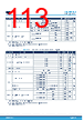
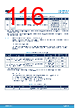
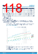
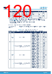
117 / 238 page  6.3.15 I/O current injection characteristics As a general rule, a current injection to the I/O pins, due to external voltage below VSS or above VDD (for standard, 3.3 V-capable I/O pins) should be avoided during the normal product operation. However, in order to give an indication of the robustness of the microcontroller in cases when an abnormal injection accidentally happens, susceptibility tests are performed on a sample basis during the device characterization. Functional susceptibility to I/O current injection While a simple application is executed on the device, the device is stressed by injecting current into the I/O pins programmed in floating input mode. While current is injected into the I/O pin, one at a time, the device is checked for functional failures. The failure is indicated by an out of range parameter: ADC error above a certain limit (higher than 5 LSB TUE), out of conventional limits of induced leakage current on adjacent pins (out of –5 µA/+0 µA range), or other functional failure (for example reset, oscillator frequency deviation). The following tables are the compilation of the SIC1/SIC2 and functional ESD results. Negative induced A negative induced leakage current is caused by negative injection and positive induced leakage current by positive injection. Table 64. I/O current injection susceptibility Symbol Description Functional susceptibility Unit Negative injection Positive injection IINJ PF2, PI12 0 NA mA PG1, PE9, PB0, PA7, PC4, PC5, PE7, PE8, PA4, PA5, PA6, PF2, PI12, PC2_C, PC3_C, PA0_C, PA1_C, BOOT0 0 0 All other I/Os 5 NA 6.3.16 I/O port characteristics General input/output characteristics Unless otherwise specified, the parameters given in Table 65. I/O static characteristics are derived from tests performed under the conditions summarized in Table 22. General operating conditions. All I/Os are CMOS and TTL compliant (except for BOOT0). Note: For information on GPIO configuration, refer to the application note AN4899 “STM32 GPIO configuration for hardware settings and low-power consumption” available from the ST website www.st.com. Table 65. I/O static characteristics Symbol Parameter Condition Min Typ Max Unit VIL I/O input low-level voltage except BOOT0 1.62 V < VDDIOx < 3.6 V - - 0.3VDD (1) V I/O input low-level voltage except BOOT0 - - 0.4VDD−0.1(2) BOOT0 I/O input low level voltage - - 0.19VDD+0.1(2) VIH I/O input high level voltage except BOOT0 1.62 V < VDDIOx < 3.6 V 0.7VDD (1) - - V I/O input high level voltage except BOOT0 0.47VDD+0.25(2) - - BOOT0 I/O input high level voltage 0.17VDD+0.6(2) - - VHYS(2) TT_xx, FT_xxx and NRST I/O input hysteresis 1.62 V < VDDIOx < 3.6 V - 250 - mV BOOT0 I/O input hysteresis - 200 - Ilkg FT_xx input leakage current(2) 0 < VIN ≤ Max(VDDxxx)(5) - - ±250 nA Max(VDDxxx) < VIN ≤ 5.5 V (3)(4)(5) - - 1500 FT_u I/O 0 < VIN ≤ Max(VDDxxx)(5) - - ±350 STM32H7B3xI Operating conditions DS13139 - Rev 8 page 117/238 |
|
Enlace URL |
| ¿ALLDATASHEET es útil para Ud.? [ DONATE ] |
Todo acerca de Alldatasheet | Publicidad | Contáctenos | Política de Privacidad | Enlace a la hoja de datos | Intercambio de Enlaces | Lista de Fabricantes All Rights Reserved©Alldatasheet.com |
| Russian : Alldatasheetru.com | Korean : Alldatasheet.co.kr | Spanish : Alldatasheet.es | French : Alldatasheet.fr | Italian : Alldatasheetit.com Portuguese : Alldatasheetpt.com | Polish : Alldatasheet.pl | Vietnamese : Alldatasheet.vn Indian : Alldatasheet.in | Mexican : Alldatasheet.com.mx | British : Alldatasheet.co.uk | New Zealand : Alldatasheet.co.nz |
|
Family Site : ic2ic.com |
icmetro.com |
 Mexican ▼
 English
 Chinese
 German
 Japanese
 Russian
 Korean
 Spanish
 French
 Italian
 Portuguese
 Polish
 Vietnamese
 Indian
 Mexican
 British
 New Zealand