|
Motor de Búsqueda de Datasheet de Componentes Electrónicos |
|
|
Motor de Búsqueda de Datasheet de Componentes Electrónicos |
|
ADRF6655ACPZ-R7 Datasheet(PDF) 20 Page - Analog Devices |
|
|
|||||||||||||||||||||||||||||
ADRF6655ACPZ-R7 Datasheet(HTML) 20 Page - Analog Devices |
|
|
20 / 44 page 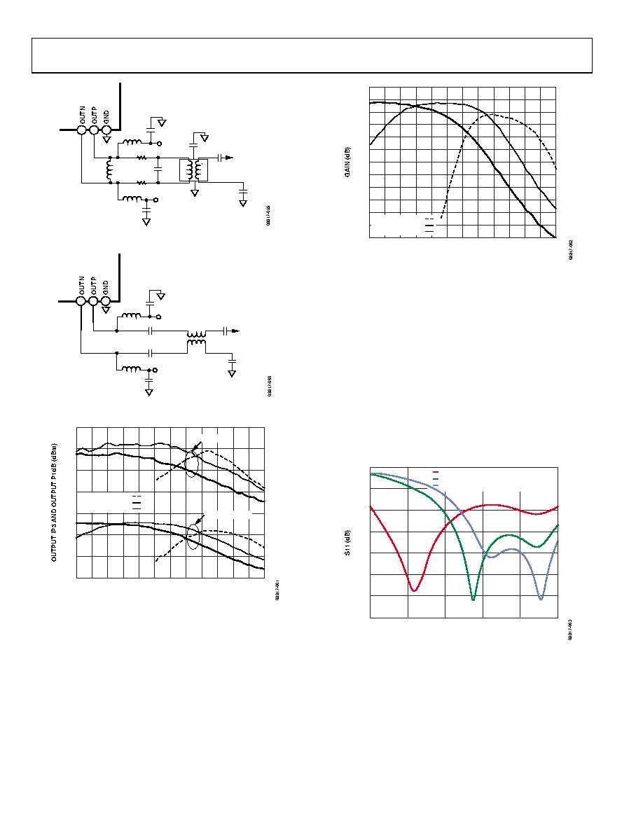 ADRF6655 Rev. 0 | Page 20 of 44 ADRF6655 T6 1600MHz OUTPUT INTERFACE VCC 1.5pF 15nH 0 Ω 36nH VCC 36nH IF OUT 1nF 150pF 1nF 150pF 1nF 0 Ω ANAREN BD1722J50200A00 18 19 20 Figure 57. 1600 MHz Output Matching Network (Output return loss measured to be better than 12 dB from 1400 MHz to 1680 MHz.) ADRF6655 T3 2100MHz OUTPUT INTERFACE VCC VCC 27nH 0603CS 27nH 0603CS IF OUT 1nF 150pF 3pF 3pF 1nF 150pF TC1-1-13M+ 18 19 20 Figure 58. 2100 MHz Output Matching Network (Output return loss measured to be better than 12 dB from 2000 MHz to 2200 MHz.) 0 5 10 15 20 25 30 35 0.7 0.8 0.9 1.0 1.1 1.2 1.3 1.4 1.5 1.6 1.7 1.8 1.9 OUTPUT FREQUENCY (GHz) 900MHz MATCH 1200MHz MATCH 1600MHz MATCH OUTPUT P1dB OUTPUT IP3 Figure 59. Measured Output Linearity for 900 MHz, 1200 MHz, and 1600 MHz Matching Networks (See Figure 54, Figure 55, and Figure 57 for Implementation) 0.7 0.8 0.9 1.0 1.1 1.2 1.3 1.4 1.5 1.6 1.7 1.8 1.9 OUTPUT FREQUENCY (GHz) –10 –9 –8 –7 –6 –5 –4 –3 –2 –1 0 1 2 900MHz MATCH 1200MHz MATCH 1600MHz MATCH Figure 60. Measured Conversion Gain for 900 MHz, 1200 MHz, and 1600 MHz Matching Networks (See Figure 54, Figure 55, and Figure 57 for Implementation) INPUT MATCHING The ADRF6655 uses a balanced 50 Ω input impedance to help simplify external connections. For low loss interfacing, the driving source should be transformed to present a balanced 50 Ω source impedance. An appropriate 1:1 impedance ratio input balun should be used when attempting to interface to an unbalanced 50 Ω source. For input frequencies below ~1.5 GHz, the TC1-1-13M+ from Mini-Circuits or similar baluns should provide good return loss and maximum power gain. For higher frequencies, baluns, such as the TC1-1-43A+, are recommended for lowest insertion loss. The ac coupling capacitors can be optimized with the balun to provide optimum input match. A few examples are provided in Figure 61 for a range of different IF output frequencies. –35 –30 –25 –20 –15 –10 –5 0 0.5 1.0 1.5 2.0 2.5 3.0 FREQUENCY (GHz) TC1-1-43A+ WITH 10pF AC COUPLING TC1-1-43A+ WITH 3pF AC COUPLING TC1-1-43A+ WITH 1.8pF AC COUPLING Figure 61. Measured RF Input Return Loss Using the TC1-1-43A+ 1:1 Balun (Plotted for Several AC Coupling Capacitor Values) It is also possible to use lumped element LC lattice networks to transform an unbalanced source into a balanced source at the mixer input pins. In either case, the mixer input pins should be dc blocked using adequately sized series capacitors. |
|
Enlace URL |
| ¿ALLDATASHEET es útil para Ud.? [ DONATE ] |
Todo acerca de Alldatasheet | Publicidad | Contáctenos | Política de Privacidad | Enlace a la hoja de datos | Intercambio de Enlaces | Lista de Fabricantes All Rights Reserved©Alldatasheet.com |
| Russian : Alldatasheetru.com | Korean : Alldatasheet.co.kr | Spanish : Alldatasheet.es | French : Alldatasheet.fr | Italian : Alldatasheetit.com Portuguese : Alldatasheetpt.com | Polish : Alldatasheet.pl | Vietnamese : Alldatasheet.vn Indian : Alldatasheet.in | Mexican : Alldatasheet.com.mx | British : Alldatasheet.co.uk | New Zealand : Alldatasheet.co.nz |
|
Family Site : ic2ic.com |
icmetro.com |
 Mexican ▼
 English
 Chinese
 German
 Japanese
 Russian
 Korean
 Spanish
 French
 Italian
 Portuguese
 Polish
 Vietnamese
 Indian
 Mexican
 British
 New Zealand