|
Motor de Búsqueda de Datasheet de Componentes Electrónicos |
|
|
Motor de Búsqueda de Datasheet de Componentes Electrónicos |
|
AD623 Datasheet(PDF) 16 Page - Analog Devices |
|
|
|||||||||||||||||||||||||||||
AD623 Datasheet(HTML) 16 Page - Analog Devices |
|
|
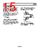
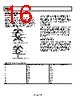
16 / 24 page  AD623 Rev. D | Page 16 of 24 APPLICATIONS INFORMATION BASIC CONNECTION Figure 42 and Figure 43 show the basic connection circuits for the AD623. The +VS and −VS terminals are connected to the power supply. The supply can be either bipolar (VS = ±2.5 V to ±6 V) or single supply (−VS = 0 V, +VS = 3.0 V to 12 V). Power supplies should be capacitively decoupled close to the power pins of the device. For the best results, use surface-mount 0.1 μF ceramic chip capacitors and 10 μF electrolytic tantalum capacitors. RG RG VIN OUTPUT VOUT REF RG REF (INPUT) +2.5V TO +6V +VS 10µF 0.1µF –2.5V TO –6V –VS 10µF 0.1µF Figure 42. Dual-Supply Basic Connection RG RG VIN OUTPUT VOUT REF RG REF (INPUT) +3V TO +12V +VS 10µF 0.1µF Figure 43. Single-Supply Basic Connection The input voltage, which can be either single-ended (tie either −IN or +IN to ground), or differential is amplified by the programmed gain. The output signal appears as the voltage difference between the OUTPUT pin and the externally applied voltage on the REF input. For a ground-referenced output, REF should be grounded. GAIN SELECTION The gain of the AD623 is resistor programmed by RG, or more precisely, by whatever impedance appears between Pin 1 and Pin 8. The AD623 is designed to offer accurate gains using 0.1% to 1% tolerance resistors. Table 5 shows the required values of RG for the various gains. Note that for G = 1, the RG terminals are unconnected (RG = ∞). For any arbitrary gain, RG can be calculated by RG = 100 kΩ/(G − 1) REFERENCE TERMINAL The reference terminal potential defines the zero output voltage and is especially useful when the load does not share a precise ground with the rest of the system. It provides a direct means of injecting a precise offset to the output. The reference terminal is also useful when bipolar signals are being amplified because it can be used to provide a virtual ground voltage. The voltage on the reference terminal can be varied from −VS to +VS. Table 5. Required Values of Gain Resistors Desired Gain 1% Standard Table Value of RG (Ω) Calculated Gain Using 1% Resistors 2 100 k 2 5 24.9 k 5.02 10 11 k 10.09 20 5.23 k 20.12 33 3.09 k 33.36 40 2.55 k 40.21 50 2.05 k 49.78 65 1.58 k 64.29 100 1.02 k 99.04 200 499 201.4 500 200 501 1000 100 1001 |
|
|
Enlace URL |
| ¿ALLDATASHEET es útil para Ud.? [ DONATE ] |
Todo acerca de Alldatasheet | Publicidad | Contáctenos | Política de Privacidad | Enlace a la hoja de datos | Intercambio de Enlaces | Lista de Fabricantes All Rights Reserved©Alldatasheet.com |
| Russian : Alldatasheetru.com | Korean : Alldatasheet.co.kr | Spanish : Alldatasheet.es | French : Alldatasheet.fr | Italian : Alldatasheetit.com Portuguese : Alldatasheetpt.com | Polish : Alldatasheet.pl | Vietnamese : Alldatasheet.vn Indian : Alldatasheet.in | Mexican : Alldatasheet.com.mx | British : Alldatasheet.co.uk | New Zealand : Alldatasheet.co.nz |
|
Family Site : ic2ic.com |
icmetro.com |
 Mexican ▼
 English
 Chinese
 German
 Japanese
 Russian
 Korean
 Spanish
 French
 Italian
 Portuguese
 Polish
 Vietnamese
 Indian
 Mexican
 British
 New Zealand