|
Motor de Búsqueda de Datasheet de Componentes Electrónicos |
|
|
Motor de Búsqueda de Datasheet de Componentes Electrónicos |
|
AD623 Datasheet(PDF) 18 Page - Analog Devices |
|
|
|||||||||||||||||||||||||||||
AD623 Datasheet(HTML) 18 Page - Analog Devices |
|
|
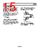
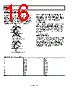
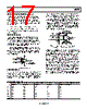
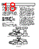
18 / 24 page  AD623 Rev. D | Page 18 of 24 The circuit in Figure 45 should be built using a PC board with a ground plane on both sides. All component leads should be as short as possible. Resistors R1 and R2 can be common 1% metal film units, but Capacitors C1 and C2 need to be ±5% tolerance devices to avoid degrading the circuit’s common-mode rejection. Either the traditional 5% silver mica units or Panasonic ±2% PPS film capacitors are recommended. In many applications, shielded cables are used to minimize noise; for best CMR over frequency, the shield should be properly driven. Figure 46 shows an active guard driver that is configured to improve ac common-mode rejection by bootstrapping the capacitances of input cable shields, thus minimizing the capacitance mismatch between the inputs. AD623 OUTPUT REF +VS –VS 2 1 8 3 6 5 7 4 RG 2 RG 2 AD8031 100Ω –IN +IN Figure 46. Common-Mode Shield Driver GROUNDING Because the AD623 output voltage is developed with respect to the potential on the reference terminal, many grounding problems can be solved by simply tying the REF pin to the appropriate local ground. The REF pin should, however, be tied to a low impedance point for optimal CMR. The use of ground planes is recommended to minimize the impedance of ground returns (and hence the size of dc errors). To isolate low level analog signals from a noisy digital environment, many data acquisition components have separate analog and digital ground returns (see Figure 47). All ground pins from mixed signal components, such as analog-to-digital converters (ADCs), should be returned through the high quality analog ground plane. Maximum isolation between analog and digital is achieved by connecting the ground planes back at the supplies. The digital return currents from the ADC that flow in the analog ground plane, in general, have a negligible effect on noise performance. If there is only a single power supply available, it must be shared by both digital and analog circuitry. Figure 48 shows how to minimize interference between the digital and analog circuitry. As in the previous case, separate analog and digital ground planes should be used (reasonably thick traces can be used as an alternative to a digital ground plane). These ground planes should be connected at the ground pin of the power supply. Separate traces should be run from the power supply to the supply pins of the digital and analog circuits. Ideally, each device should have its own power supply trace, but these can be shared by a number of devices, as long as a single trace is not used to route current to both digital and analog circuitry. AGND VDD MICROPROCESSOR AD623 2 3 6 5 7 4 ANALOG POWER SUPPLY GND –5V +5V DIGITAL POWER SUPPLY +5V GND 4 VIN1 1 VDD 6 AGND 14 DGND 3 VIN2 ADC AD7892-2 0.1µF 0.1µF 0.1µF 0.1µF 12 Figure 47. Optimal Grounding Practice for a Bipolar Supply Environment with Separate Analog and Digital Supplies AGND VDD MICROPROCESSOR AD623 2 3 6 5 7 4 4 VIN1 1 VDD 6 AGND 14 DGND ADC AD7892-2 0.1µF 0.1µF 0.1µF 12 POWER SUPPLY +5V GND Figure 48. Optimal Ground Practice in a Single Supply Environment |
|
|
Enlace URL |
| ¿ALLDATASHEET es útil para Ud.? [ DONATE ] |
Todo acerca de Alldatasheet | Publicidad | Contáctenos | Política de Privacidad | Enlace a la hoja de datos | Intercambio de Enlaces | Lista de Fabricantes All Rights Reserved©Alldatasheet.com |
| Russian : Alldatasheetru.com | Korean : Alldatasheet.co.kr | Spanish : Alldatasheet.es | French : Alldatasheet.fr | Italian : Alldatasheetit.com Portuguese : Alldatasheetpt.com | Polish : Alldatasheet.pl | Vietnamese : Alldatasheet.vn Indian : Alldatasheet.in | Mexican : Alldatasheet.com.mx | British : Alldatasheet.co.uk | New Zealand : Alldatasheet.co.nz |
|
Family Site : ic2ic.com |
icmetro.com |
 Mexican ▼
 English
 Chinese
 German
 Japanese
 Russian
 Korean
 Spanish
 French
 Italian
 Portuguese
 Polish
 Vietnamese
 Indian
 Mexican
 British
 New Zealand