|
Motor de Búsqueda de Datasheet de Componentes Electrónicos |
|
|
Motor de Búsqueda de Datasheet de Componentes Electrónicos |
|
AD623 Datasheet(PDF) 20 Page - Analog Devices |
|
|
|||||||||||||||||||||||||||||
AD623 Datasheet(HTML) 20 Page - Analog Devices |
|
|
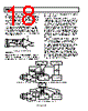
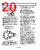
20 / 24 page  AD623 Rev. D | Page 20 of 24 Amplifying Signals with Low Common-Mode Voltage Because the common-mode input range of the AD623 extends 0.1 V below ground, it is possible to measure small differential signals which have low, or no, common-mode component. Figure 54 shows a thermocouple application where one side of the J-type thermocouple is grounded. 5V 0.1µF AD623 RG 1.02kΩ REF J-TYPE THERMOCOUPLE OUTPUT 2V Figure 54. Amplifying Bipolar Signals with Low Common-Mode Voltage Over a temperature range of −200°C to +200°C, the J-type thermo- couple delivers a voltage ranging from −7.890 mV to +10.777 mV. A programmed gain on the AD623 of 100 (RG = 1.02 kΩ) and a voltage on the REF pin of 2 V, results in the output voltage ranging from 1.110 V to 3.077 V relative to ground. INPUT DIFFERENTIAL AND COMMON-MODE RANGE vs. SUPPLY AND GAIN Figure 55 shows a simplified block diagram of the AD623. The voltages at the outputs of Amplifier A1 and Amplifier A2 are given by VA2 = VCM + VDIFF/2 + 0.6 V + VDIFF × RF/RG = VCM + 0.6 V + VDIFF × Gain/2 VA1 = VCM + VDIFF/2 + 0.6 V + VDIFF × RF/RG = VCM + 0.6 V − VDIFF × Gain/2 POSITIVE SUPPLY 7 4 INVERTING 2 7 4 NEGATIVE SUPPLY NONINVERTING 3 RF 50kΩ 50kΩ 50kΩ RF 50kΩ 50kΩ 50kΩ OUTPUT 6 REF 5 8 1 GAIN RG A1 A2 A3 VDIFF 2 – + VDIFF 2 – + VCM Figure 55. Simplified Block Diagram The voltages on these internal nodes are critical in determining whether the output voltage will be clipped. The VA1 and VA2 voltages can swing from approximately 10 mV above the negative supply (V− or ground) to within approximately 100 mV of the positive rail before clipping occurs. Based on this and from the previous equations, the maximum and minimum input common-mode voltages are given by the following equations: VCMMAX = V+ − 0.7 V − VDIFF × Gain/2 VCMMIN = V− − 0.590 V + VDIFF × Gain/2 These equations can be rearranged to give the maximum possible differential voltage (positive or negative) for a particular common-mode voltage, gain, and power supply. Because the signals on A1 and A2 can clip on either rail, the maximum differential voltage are the lesser of the two equations. |VDIFFMAX| = 2 (V+ − 0.7 V − VCM/Gain |VDIFFMAX| = 2 (VCM − V− +0.590 V/Gain However, the range on the differential input voltage range is also constrained by the output swing. Therefore, the range of VDIFF may have to be lower according the following equation. Input Range ≤ Available Output Swing/Gain For a bipolar input voltage with a common-mode voltage that is roughly half way between the rails, VDIFFMAX is half the value that the previous equations yield because the REF pin is at midsupply. Note that the available output swing is given for different supply conditions in the Specifications section. The equations can be rearranged to give the maximum gain for a fixed set of input conditions. Again, the maximum gain will be the lesser of the two equations. GainMAX = 2 (V+ − 0.7 V − VCM)/VDIFF GainMAX = 2 (VCM − V− +0.590 V)/VDIFF Again, it is recommended that the resulting gain times the input range is less than the available output swing. If this is not the case, the maximum gain is given by GainMAX = Available Output Swing/Input Range Also for bipolar inputs (that is, input range = 2 VDIFF), the maximum gain is half the value yielded by the previous equations because the REF pin must be at midsupply. The maximum gain and resulting output swing for different input conditions is given in Table 8. Output voltages are referenced to the voltage on the REF pin. For the purposes of computation, it is necessary to break down the input voltage into its differential and common-mode component. Therefore, when one of the inputs is grounded or at a fixed voltage, the common-mode voltage changes as the differential voltage changes. Take the case of the thermocouple amplifier in Figure 54. The inverting input on the AD623 is grounded; therefore, when the input voltage is −10 mV, the voltage on the noninverting input is −10 mV. For the purpose of the signal swing calculations, this input voltage should be composed of a common- mode voltage of −5 mV (that is, (+IN + −IN)/2) and a differential input voltage of −10 mV (that is, +IN − −IN). |
|
|
Enlace URL |
| ¿ALLDATASHEET es útil para Ud.? [ DONATE ] |
Todo acerca de Alldatasheet | Publicidad | Contáctenos | Política de Privacidad | Enlace a la hoja de datos | Intercambio de Enlaces | Lista de Fabricantes All Rights Reserved©Alldatasheet.com |
| Russian : Alldatasheetru.com | Korean : Alldatasheet.co.kr | Spanish : Alldatasheet.es | French : Alldatasheet.fr | Italian : Alldatasheetit.com Portuguese : Alldatasheetpt.com | Polish : Alldatasheet.pl | Vietnamese : Alldatasheet.vn Indian : Alldatasheet.in | Mexican : Alldatasheet.com.mx | British : Alldatasheet.co.uk | New Zealand : Alldatasheet.co.nz |
|
Family Site : ic2ic.com |
icmetro.com |
 Mexican ▼
 English
 Chinese
 German
 Japanese
 Russian
 Korean
 Spanish
 French
 Italian
 Portuguese
 Polish
 Vietnamese
 Indian
 Mexican
 British
 New Zealand