|
Motor de Búsqueda de Datasheet de Componentes Electrónicos |
|
|
Motor de Búsqueda de Datasheet de Componentes Electrónicos |
|
AD623 Datasheet(PDF) 17 Page - Analog Devices |
|
|
|||||||||||||||||||||||||||||
AD623 Datasheet(HTML) 17 Page - Analog Devices |
|
|
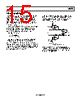
17 / 24 page  AD623 Rev. D | Page 17 of 24 INPUT AND OUTPUT OFFSET VOLTAGE The low errors of the AD623 are attributed to two sources, input and output errors. The output error is divided by the programmed gain when referred to the input. In practice, the input errors dominate at high gains and the output errors dominate at low gains. The total VOS for a given gain is calculated as the following: Total Error RTI = Input Error + (Output Error/G) Total Error RTO = (Input Error × G) + Output Error RTI offset errors and noise voltages for different gains are shown in Table 6. INPUT PROTECTION Internal supply referenced clamping diodes allow the input, reference, output, and gain terminals of the AD623 to safely withstand overvoltages of 0.3 V above or below the supplies. This is true for all gains and for power on and power off. This last case is particularly important because the signal source and amplifier may be powered separately. If the overvoltage is expected to exceed this value, the current through these diodes should be limited to about 10 mA using external current limiting resistors (see Figure 44). The size of this resistor is defined by the supply voltage and the required overvoltage protection. RG VOVER VOVER AD623 OUTPUT +VS –VS RLIM RLIM I = 10mA MAX RLIM = VOVER –VS + 0.7V 10mA Figure 44. Input Protection RF INTERFERENCE All instrumentation amplifiers can rectify high frequency out- of-band signals. Once rectified, these signals appear as dc offset errors at the output. The circuit in Figure 45 provides good RFI suppression without reducing performance within the pass band of the in-amp. Resistor R1 and Capacitor C1 (and likewise, R2 and C2) form a low-pass RC filter that has a −3 dB bandwidth equal to F = 1/(2 π R1C1). Using the component values shown, this filter has a −3 dB bandwidth of approximately 40 kHz. Resistors R1 and R2 were selected to be large enough to isolate the input of the circuit from the capacitors, but not large enough to significantly increase the noise of the circuit. To preserve common-mode rejection in the amplifier’s pass band, Capacitors C1 and C2 need to be 5% or better units, or low cost 20% units can be tested and binned to provide closely matched devices. RG –IN +IN AD623 VOUT R1 4.02kΩ 1% R2 4.02kΩ 1% REFERENCE +VS 0.01µF 0.33µF +VS 0.01µF 0.33µF C1 1000pF 5% C3 0.047µF C2 1000pF 5% NOTES: 1. LOCATE C1 TO C3 AS CLOSE TO THE INPUT PINS AS POSSIBLE. Figure 45. Circuit to Attenuate RF Interference Capacitor C3 is needed to maintain common-mode rejection at the low frequencies. R1/R2 and C1/C2 form a bridge circuit whose output appears across the input pins of the in-amp. Any mismatch between C1 and C2 unbalances the bridge and reduces the common-mode rejection. C3 ensures that any RF signals are common mode (the same on both in-amp inputs) and are not applied differentially. This second low-pass network, R1 + R2 and C3, has a −3 dB frequency equal to 1/(2 π (R1 + R2) (C3)). Using a C3 value of 0.047 μF, the −3 dB signal bandwidth of this circuit is approximately 400 Hz. The typical dc offset shift over frequency is less than 1.5 μV and the circuit’s RF signal rejection is better than 71 dB. The 3 dB signal bandwidth of this circuit may be increased to 900 Hz by reducing Resistors R1 and R2 to 2.2 kΩ. The performance is similar to using 4 kΩ resistors, except that the circuitry preceding the in-amp must drive a lower impedance load. Table 6. RTI Error Sources Maximum Total Input Offset Error (μV) Maximum Total Input Offset Drift (μV/°C) Total Input Referred Noise (nV/√Hz) Gain AD623A AD623B AD623A AD623B AD623A and AD623B 1 1200 600 12 11 62 2 700 350 7 6 45 5 400 200 4 3 38 10 300 150 3 2 35 20 250 125 2.5 1.5 35 50 220 110 2.2 1.2 35 100 210 105 2.1 1.1 35 1000 200 100 2 1 35 |
|
|
Enlace URL |
| ¿ALLDATASHEET es útil para Ud.? [ DONATE ] |
Todo acerca de Alldatasheet | Publicidad | Contáctenos | Política de Privacidad | Enlace a la hoja de datos | Intercambio de Enlaces | Lista de Fabricantes All Rights Reserved©Alldatasheet.com |
| Russian : Alldatasheetru.com | Korean : Alldatasheet.co.kr | Spanish : Alldatasheet.es | French : Alldatasheet.fr | Italian : Alldatasheetit.com Portuguese : Alldatasheetpt.com | Polish : Alldatasheet.pl | Vietnamese : Alldatasheet.vn Indian : Alldatasheet.in | Mexican : Alldatasheet.com.mx | British : Alldatasheet.co.uk | New Zealand : Alldatasheet.co.nz |
|
Family Site : ic2ic.com |
icmetro.com |
 Mexican ▼
 English
 Chinese
 German
 Japanese
 Russian
 Korean
 Spanish
 French
 Italian
 Portuguese
 Polish
 Vietnamese
 Indian
 Mexican
 British
 New Zealand