|
Motor de Búsqueda de Datasheet de Componentes Electrónicos |
|
|
Motor de Búsqueda de Datasheet de Componentes Electrónicos |
|
AD623 Datasheet(PDF) 19 Page - Analog Devices |
|
|
|||||||||||||||||||||||||||||
AD623 Datasheet(HTML) 19 Page - Analog Devices |
|
|
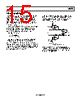
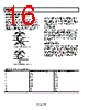
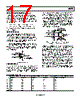
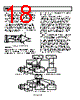
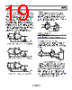
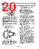
19 / 24 page  AD623 Rev. D | Page 19 of 24 Ground Returns for Input Bias Currents Input bias currents are those dc currents that must flow to bias the input transistors of an amplifier. These are usually transistor base currents. When amplifying floating input sources, such as transformers or ac-coupled sources, there must be a direct dc path into each input in order that the bias current can flow. Figure 49, Figure 50, and Figure 51 show how a bias current path can be provided for the cases of transformer coupling, thermocouple, and capacitive ac coupling. In dc-coupled resistive bridge applications, providing this path is generally not necessary as the bias current simply flows from the bridge supply through the bridge into the amplifier. However, if the impedances that the two inputs see are large and differ by a large amount (>10 kΩ), the offset current of the input stage causes dc errors proportional with the input offset voltage of the amplifier. AD623 OUTPUT TO POWER SUPPLY GROUND REF LOAD +VS –VS 2 1 8 3 6 5 7 4 RG –IN +IN Figure 49. Ground Returns for Bias Currents with Transformer-Coupled Inputs AD623 OTUPUT TO POWER SUPPLY GROUND REF LOAD +VS –VS 2 1 8 3 6 5 7 4 RG –IN +IN Figure 50. Ground Returns for Bias Currents with Thermocouple Inputs AD623 OUTPUT TO POWER SUPPLY GROUND REF LOAD +VS –VS 2 1 8 3 6 5 7 4 RG –IN +IN 100kΩ 100kΩ Figure 51. Ground Returns for Bias Currents with AC-Coupled Inputs Output Buffering The AD623 is designed to drive loads of 10 kΩ or greater. If the load is less than this value, the output of the AD623 should be buffered with a precision single-supply op amp, such as the OP113. This op amp can swing from 0 V to 4 V on its output while driving a load as small as 600 Ω. Table 7 summarizes the performance of some buffer op amps. 5V 0.1µF 5V 0.1µF AD623 OP113 RG VIN REFERENCE VOUT Figure 52. Output Buffering Table 7. Buffering Options Op Amp Description OP113 Single supply, high output current OP191 Rail-to-rail input and output, low supply current Single-Supply Data Acquisition System Interfacing bipolar signals to single-supply ADCs presents a challenge. The bipolar signal must be mapped into the input range of the ADC. Figure 53 shows how this translation can be achieved. 5V 0.1µF 5V 5V 0.1µF AD623 RG 1.02kΩ REFERENCE ±10mV AIN REFOUT REFIN AD7776 Figure 53. A Single-Supply Data Acquisition System The bridge circuit is excited by a 5 V supply. The full-scale output voltage from the bridge (±10 mV) therefore has a common- mode level of 2.5 V. The AD623 removes the common-mode component and amplifies the input signal by a factor of 100 (RGAIN = 1.02 kΩ). This results in an output signal of ±1 V. To prevent this signal from running into the ground rail of the AD623, the voltage on the REF pin must be raised to at least 1 V. In this example, the 2 V reference voltage from the AD7776 ADC is used to bias the output voltage of the AD623 to 2 V ± 1 V. This corresponds to the input range of the ADC. |
|
|
Enlace URL |
| ¿ALLDATASHEET es útil para Ud.? [ DONATE ] |
Todo acerca de Alldatasheet | Publicidad | Contáctenos | Política de Privacidad | Enlace a la hoja de datos | Intercambio de Enlaces | Lista de Fabricantes All Rights Reserved©Alldatasheet.com |
| Russian : Alldatasheetru.com | Korean : Alldatasheet.co.kr | Spanish : Alldatasheet.es | French : Alldatasheet.fr | Italian : Alldatasheetit.com Portuguese : Alldatasheetpt.com | Polish : Alldatasheet.pl | Vietnamese : Alldatasheet.vn Indian : Alldatasheet.in | Mexican : Alldatasheet.com.mx | British : Alldatasheet.co.uk | New Zealand : Alldatasheet.co.nz |
|
Family Site : ic2ic.com |
icmetro.com |
 Mexican ▼
 English
 Chinese
 German
 Japanese
 Russian
 Korean
 Spanish
 French
 Italian
 Portuguese
 Polish
 Vietnamese
 Indian
 Mexican
 British
 New Zealand