|
Motor de Búsqueda de Datasheet de Componentes Electrónicos |
|
|
Motor de Búsqueda de Datasheet de Componentes Electrónicos |
|
AD7011 Datasheet(PDF) 9 Page - Analog Devices |
|
|
|||||||||||||||||||||||||||||
AD7011 Datasheet(HTML) 9 Page - Analog Devices |
|
|
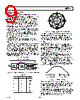
9 / 12 page  AD7011 REV. B –9– I Q Figure 10. π/4 DQPSK Constellation Diagram Figure 10 illustrates the π/4 DQPSK constellation diagram as described above, showing the eight possible states for [Ik, Qk]. The Ik and Qk impulses are then filtered by FIR raised root cosine filters ( α = 0.35), generating 10-bit I and Q data. The FIR root raised cosine filters have an impulse response of ±4 symbols. Transmit Calibration When the transmit section is brought out of sleep mode (POWER high), the transmit section initiates a self-calibration routine to remove the offset between ITx and ITx and an offset between QTx and QTx. READY goes high on the completion of the self-calibration routine. Once READY goes high, BIN (Burst In) can be brought high to initiate a transmit burst. Ramp-Up/Down Envelope Logic The AD7011 provides on-chip envelope shaping logic, providing power shaping control for the beginning and end of a transmit burst. When BIN (Burst In) is brought high, the modulator is reset to a transmitting all zeros state (i.e., Xk = Yk = 0) and continues to transmit all zeros for the first three symbols, during which the ramp-up envelope goes from zero to full scale as illustrated in Figure 11. The next symbol to be transmitted is [I1, Q1], which represents the first two data bits clocked in after BIN going high, i.e., [X1, Y1]. –– – –– COS π ––– 1 2 1 2 t 3T –– + –– COS π ––– 1 2 1 2 t 3T 3 SYMBOLS 3 SYMBOLS Figure 11. Ramp Envelope When BIN is brought low, indicating the end of a transmit burst, the current Di-bit symbol [XN+4, YN+4] that the AD7011 is receiving will be the last symbol to be computed for the four symbol ramp-down sequence. Also the N th symbol is the last active symbol prior to ramping down. However, because the impulse response is equal to ±4 symbols, four additional symbols are required to fully compute the analog outputs when transmitting the (N+4) th symbol. Hence there will be eight subsequent TxCLKs, latching four additional Di-bit symbols: [XN + 5, YN + 5] to [XN + 8, YN + 8]. CIRCUIT DESCRIPTION TRANSMIT SECTION The transmit section of the AD7011 generates π/4 DQPSK I and Q waveforms in accordance with TIA specification. This is accomplished by a digital π/4 DQPSK modulator, which includes the root-raised cosine filters ( α = 0.35), followed by two 10-bit DACs and on-chip reconstruction filters. The π/4 DQPSK (Differential Quadrature Phase Shift Keying) digital modulator generates 10-bit I and Q data in response to the transmit data stream. The 10-bit I and Q DACs are filtered by on-chip reconstruction filters, which also generate differential analog outputs for both I and Q channels. The AD7011 transmit channel also provides an analog mode, where direct access to the I and Q DACs is provided, bypassing the π/4 DQPSK modulator. This is provided so that the AD7011 transmit channel can also be used to perform the conversion and filtering of the analog waveforms required to emulate the existing analog cellular system. /4 DQPSK Modulator The π/4 DQPSK modulator generates 10-bit I and Q data (Inphase and Quadrature) which are loaded into the I and Q 10-bit transmit DACs. Figure 9 shows the functional block diagram of the π/4 DQPSK modulator. The transmit serial data (TxDATA) is first con- verted into Di-bit symbols [Xk, Yk], using a 2-bit serial to parallel converter. The data is then differentially encoded; symbols are transmitted as changes in phase rather than absolute phases. Each symbol represents a phase change, as illustrated in Table III, and this along with the previously transmitted symbol determines the next symbol to be transmitted. The differential phase encoder generates I and Q impulses [Ik, Qk] in response to the Di-bit symbols according to: Ik = COS [φk–1 + ∆φk] Qk = SIN [φk–1 + ∆φk] DIFFERENTIAL PHASE ENCODER ROOT-RAISED COSINE FILTER I DATA Q DATA 10 10 2-BIT SERIAL TO PARALLEL CONVERTER π /4 DQPSK DIGITAL MODULATOR X k Y k I k Q k ROOT-RAISED COSINE FILTER TxDATA Figure 9. π/4 DQPSK Modulator Functional Block Diagram Table III. Xk Yk ∆ k 11 −3π 4 01 3 π 4 00 π 4 10 −π 4 |
|
|
Enlace URL |
| ¿ALLDATASHEET es útil para Ud.? [ DONATE ] |
Todo acerca de Alldatasheet | Publicidad | Contáctenos | Política de Privacidad | Enlace a la hoja de datos | Intercambio de Enlaces | Lista de Fabricantes All Rights Reserved©Alldatasheet.com |
| Russian : Alldatasheetru.com | Korean : Alldatasheet.co.kr | Spanish : Alldatasheet.es | French : Alldatasheet.fr | Italian : Alldatasheetit.com Portuguese : Alldatasheetpt.com | Polish : Alldatasheet.pl | Vietnamese : Alldatasheet.vn Indian : Alldatasheet.in | Mexican : Alldatasheet.com.mx | British : Alldatasheet.co.uk | New Zealand : Alldatasheet.co.nz |
|
Family Site : ic2ic.com |
icmetro.com |
 Mexican ▼
 English
 Chinese
 German
 Japanese
 Russian
 Korean
 Spanish
 French
 Italian
 Portuguese
 Polish
 Vietnamese
 Indian
 Mexican
 British
 New Zealand