|
Motor de Búsqueda de Datasheet de Componentes Electrónicos |
|
|
Motor de Búsqueda de Datasheet de Componentes Electrónicos |
|
AD7011 Datasheet(PDF) 10 Page - Analog Devices |
|
|
|||||||||||||||||||||||||||||
AD7011 Datasheet(HTML) 10 Page - Analog Devices |
|
|
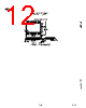
10 / 12 page  AD7011 REV. B –10– As Figure 12 illustrates, the ramp-down envelope reaches zero after three symbols, hence the fourth symbol does not actually get transmitted. Reconstruction Filters The reconstruction filters smooth the DAC output signals, providing continuous time I and Q waveforms at the output pins. These are 4th order Bessel low-pass filters with a –3 dB frequency of approximately 25 kHz. The filters are designed to have a linear phase response in the passband and due to the reconstruction filters being on-chip, the phase mismatch between the I and Q transmit channels is kept to a minimum. Transmit Section Digital Interface MODE1 = MODE2 = DGND: Digital π/4 DQPSK Mode Figures 4 and 5 shows the timing diagrams for the transmit interface when operating in TIA π/4 DQPSK mode. POWER is sampled on the rising edge of MCLK. When POWER is brought high, the transmit section is brought out of sleep mode and initiates a self-calibration routine as described above. Once the self-calibration is complete, the READY signal goes high to indicate that a transmit burst can now begin. BIN (Burst in) is brought high to initiate a transmit burst and should only be brought high if the READY signal is already high. When BIN goes high, the READY signal goes low on the next rising edge of MCLK and TxCLK becomes active after a further three MCLK cycles. TxCLK can be used to clock out the transmit data from the ASIC or DSP on the rising edge of TxCLK and the AD7011 will latch TxDATA on the falling edge of TxCLK. When BIN is brought low, the AD7011 will continue to clock in the current Di-bit symbol (XN + 4, YN + 4) and will continue for a further 8 TxCLK cycles (four symbols). After the final TxCLK, READY goes high waiting for BIN to be brought high to begin the next transmit burst. X 1 X N Y N Y N+1 X N+1 Y N+2 X N+2 Y N+3 X N+3 Y N+4 X N+4 3 SYMBOL RAMP-UP ENVELOPE 3 SYMBOL RAMP-DOWN ENVELOPE I 1 Q 1 I N Q N I N+1 Q N+1 I N+2 Q N+2 I N+3 Q N+3 I N+4 Q N+4 0 0 0 0 SYMBOL PHASE MAX EFFECT = 480 t 1 BIN TxCLK TxDATA BOUT (ITx–ITx), (QTx–QTx) Y N+5 X N+5 Y N+6 X N+6 Y N+7 X N+7 Y N+8 X N+8 0 0 Y 1 Figure 12. Transmit Burst When POWER is brought low this puts the transmit section into a low power sleep mode, drawing minimal current. The analog outputs go high impedance while in low power sleep mode. MODE1 = VDD; MODE2 = DGND: Analog Mode Figure 6 shows the timing diagram for the transmit interface when operating in analog mode. In this mode the π/4 DQPSK modulator is bypassed and direct access to the I and Q 10-bit DACs is provided. Loading of the I and Q DACs is accom- plished using a 4 wire 16-bit serial interface. The pins TxCLK, TxDATA and BIN are all reconfigured as inputs, with the functions of FRAME, IDATA and QDATA respectively. I and Q data are loaded via the IDATA and QDATA pins and FRAME synchronizes the loading of the 16-bit I and Q words. FRAME should be brought high one clock cycle prior to the I and Q MSBs. Data is latched on the rising edge of MCLK, MSB first, where only the first 10 data bits are significant. Con- tinuous updating of the I and Q DACs is required at a rate of MCLK/16. MODE1 = DGND; MODE2 = VDD: Frequency Test Mode A special FTEST (Frequency TEST) mode is provided for the customer, where no phase modulation takes place and the mod- ulator outputs remain static. ITx is set to zero and QTx is set to full scale as Figure 7 illustrates. However, the normal ramp-up/ down envelope is still applied during the beginning and end of a burst. MODE1 = MODE2 = VDD: Factory Test Mode This mode is reserved for factory test only and should not be used by the customer for correct device operation. |
|
|
Enlace URL |
| ¿ALLDATASHEET es útil para Ud.? [ DONATE ] |
Todo acerca de Alldatasheet | Publicidad | Contáctenos | Política de Privacidad | Enlace a la hoja de datos | Intercambio de Enlaces | Lista de Fabricantes All Rights Reserved©Alldatasheet.com |
| Russian : Alldatasheetru.com | Korean : Alldatasheet.co.kr | Spanish : Alldatasheet.es | French : Alldatasheet.fr | Italian : Alldatasheetit.com Portuguese : Alldatasheetpt.com | Polish : Alldatasheet.pl | Vietnamese : Alldatasheet.vn Indian : Alldatasheet.in | Mexican : Alldatasheet.com.mx | British : Alldatasheet.co.uk | New Zealand : Alldatasheet.co.nz |
|
Family Site : ic2ic.com |
icmetro.com |
 Mexican ▼
 English
 Chinese
 German
 Japanese
 Russian
 Korean
 Spanish
 French
 Italian
 Portuguese
 Polish
 Vietnamese
 Indian
 Mexican
 British
 New Zealand