|
Motor de Búsqueda de Datasheet de Componentes Electrónicos |
|
|
Motor de Búsqueda de Datasheet de Componentes Electrónicos |
|
LTC1735CF Datasheet(PDF) 26 Page - Linear Technology |
|
|
|||||||||||||||||||||||||||||
LTC1735CF Datasheet(HTML) 26 Page - Linear Technology |
|
|
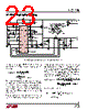
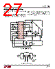
26 / 32 page  26 LTC1735 1735fc APPLICATIO S I FOR ATIO Next verify the minimum on-time of 200ns is not violated. The minimum on-time occurs at maximum VIN: t V Vf V V kHz ns ON MIN OUT IN MAX () () . () == = 18 22 300 273 Since the output voltage is below 2.4V the output resistive divider will need to be sized to not only set the output voltage but also to absorb the sense pin current. Rk V VV k V VV k MAX OUT 124 08 24 24 08 24 18 32 () . .– . .– . = = = Choosing 1% resistors: R1 = 25.5k and R2 = 32.4k yields an output voltage of 1.816V. The power dissipation on the topside MOSFET can be easily estimated. Choosing a Siliconix Si4412ADY results in RDS(ON) = 0.035Ω, CRSS = 100pF. At maximum input voltage with T(estimated) = 50 °C: P V V CC V A pF kHz mW MAIN = () +° ° [] Ω () + () ( )( )( ) = 18 22 5 1 0 005 50 25 0 035 1 7 22 5 100 300 204 2 2 . ( . )( – ) . . Because the duty cycle of the bottom MOSFET is much greater than the top, a larger MOSFET, Siliconix Si4410DY, (RDS(ON) = 0.02Ω) is chosen. The power dissipation in the bottom MOSFET, again assuming TA = 50°C, is: P VV V A mW SYNC = () ( ) Ω () = 22 1 8 22 51 1 0 02 505 2 –. .. Thanks to current foldback, the bottom MOSFET dissipa- tion in short-circuit will be less than under full load conditions. CIN is chosen for an RMS current rating of at least 2.5A at temperature. COUT is chosen with an ESR of 0.02Ω for low output ripple. The output ripple in continuous mode will be highest at the maximum input voltage. The worst-case output voltage ripple due to ESR is approximately: VR I A mV ORIPPLE ESR L P P == Ω = − () . ( . ) ∆ 002 2 3 46 PC Board Layout Checklist When laying out the printed circuit board, the following checklist should be used to ensure proper operation of the LTC1735. These items are also illustrated graphically in the layout diagram of Figure 12. Check the following in your layout: 1) Are the signal and power grounds segregated? The LTC1735 PGND pin should tie to the ground plane close to the input capacitor(s). The SGND pin should then connect to PGND, and all components that connect to SGND should make a single point tie to the SGND pin. The synchronous MOSFET source pins should connect to the input capacitor(s) ground. 2) Does the VOSENSE pin connect directly to the feedback resistors? The resistive divider R1, R2 must be connected between the (+) plate of COUT and signal ground. The 47pF to 100pF capacitor should be as close as possible to the LTC1735. Be careful locating the feedback resistors too far away from the LTC1735. The VOSENSE line should not be routed close to any other nodes with high slew rates. 3) Are the SENSE – and SENSE + leads routed together with minimum PC trace spacing? The filter capacitor between SENSE + and SENSE – should be as close as possible to the LTC1735. Ensure accurate current sensing with Kelvin connections as shown in Figure 13. Series resistance can be added to the SENSE lines to increase noise rejection. 4) Does the (+) terminal of CIN connect to the drain of the topside MOSFET(s) as closely as possible? This capacitor provides the AC current to the MOSFET(s). 5) Is the INTVCC decoupling capacitor connected closely between INTVCC and the power ground pin? This capaci- tor carries the MOSFET driver peak currents. An addi- tional 1 µF ceramic capacitor placed immediately next to |
|
Enlace URL |
| ¿ALLDATASHEET es útil para Ud.? [ DONATE ] |
Todo acerca de Alldatasheet | Publicidad | Contáctenos | Política de Privacidad | Enlace a la hoja de datos | Intercambio de Enlaces | Lista de Fabricantes All Rights Reserved©Alldatasheet.com |
| Russian : Alldatasheetru.com | Korean : Alldatasheet.co.kr | Spanish : Alldatasheet.es | French : Alldatasheet.fr | Italian : Alldatasheetit.com Portuguese : Alldatasheetpt.com | Polish : Alldatasheet.pl | Vietnamese : Alldatasheet.vn Indian : Alldatasheet.in | Mexican : Alldatasheet.com.mx | British : Alldatasheet.co.uk | New Zealand : Alldatasheet.co.nz |
|
Family Site : ic2ic.com |
icmetro.com |
 Mexican ▼
 English
 Chinese
 German
 Japanese
 Russian
 Korean
 Spanish
 French
 Italian
 Portuguese
 Polish
 Vietnamese
 Indian
 Mexican
 British
 New Zealand