|
Motor de Búsqueda de Datasheet de Componentes Electrónicos |
|
|
Motor de Búsqueda de Datasheet de Componentes Electrónicos |
|
LTC1735CF Datasheet(PDF) 27 Page - Linear Technology |
|
|
|||||||||||||||||||||||||||||
LTC1735CF Datasheet(HTML) 27 Page - Linear Technology |
|
|
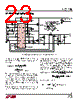
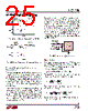
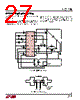
27 / 32 page 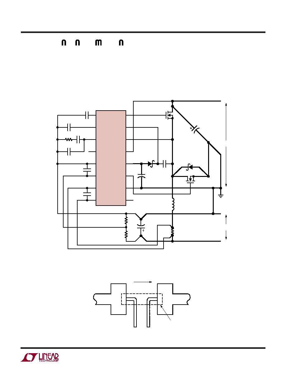 27 LTC1735 1735fc APPLICATIO S I FOR ATIO Figure 12. LTC1735 Layout Diagram Figure 13. Kelvin Sensing RSENSE the INTVCC and PGND pins can help improve noise performance. 6) Keep the switching node (SW), top gate node (TG) and boost node (BOOST) away from sensitive small-signal nodes, especially from the voltage and current sensing 16 15 14 13 12 11 10 9 1 2 3 4 5 6 7 8 COSC RUN/SS ITH FCB SGND VOSENSE SENSE– SENSE+ TG BOOST SW VIN INTVCC BG PGND EXTVCC LTC1735 CSS CC2 CC RC 47pF 1000pF COUT COSC R1 R2 CB DB RSENSE D1 M2 + 4.7 µF M1 CIN + – L1 VIN – + VOUT 1735 F12 SENSE + SENSE – HIGH CURRENT PATH 1735 F13 CURRENT SENSE RESISTOR (RSENSE) feedback pins. All of these nodes have very large and fast moving signals and therefore should be kept on the “output side” (Pin 9 to Pin 16) of the LTC1735 and occupy minimum PC trace area. |
|
Enlace URL |
| ¿ALLDATASHEET es útil para Ud.? [ DONATE ] |
Todo acerca de Alldatasheet | Publicidad | Contáctenos | Política de Privacidad | Enlace a la hoja de datos | Intercambio de Enlaces | Lista de Fabricantes All Rights Reserved©Alldatasheet.com |
| Russian : Alldatasheetru.com | Korean : Alldatasheet.co.kr | Spanish : Alldatasheet.es | French : Alldatasheet.fr | Italian : Alldatasheetit.com Portuguese : Alldatasheetpt.com | Polish : Alldatasheet.pl | Vietnamese : Alldatasheet.vn Indian : Alldatasheet.in | Mexican : Alldatasheet.com.mx | British : Alldatasheet.co.uk | New Zealand : Alldatasheet.co.nz |
|
Family Site : ic2ic.com |
icmetro.com |
 Mexican ▼
 English
 Chinese
 German
 Japanese
 Russian
 Korean
 Spanish
 French
 Italian
 Portuguese
 Polish
 Vietnamese
 Indian
 Mexican
 British
 New Zealand