|
Motor de Búsqueda de Datasheet de Componentes Electrónicos |
|
|
Motor de Búsqueda de Datasheet de Componentes Electrónicos |
|
ADP3330ARTZ-2.5-R7 Datasheet(PDF) 6 Page - Analog Devices |
|
|
|||||||||||||||||||||||||||||
ADP3330ARTZ-2.5-R7 Datasheet(HTML) 6 Page - Analog Devices |
|
|
6 / 16 page 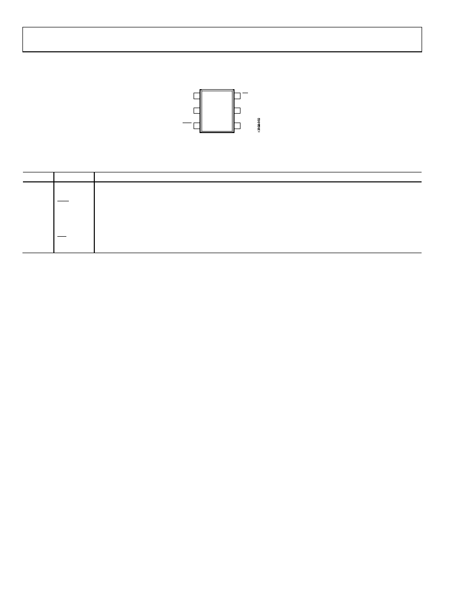 ADP3330 Data Sheet PIN CONFIGURATION AND FUNCTION DESCRIPTIONS Figure 3. Pin Configuration Table 4. Pin Function Descriptions Pin No. Mnemonic Description 1 OUT Output of the Regulator. Bypass to ground with a 0.47 µF or larger capacitor. 2 IN Regulator Input. 3 ERR Open Collector Output. This pin goes low to indicate that the output is about to go out of regulation. 4 GND Ground Pin. 5 NR Noise Reduction Pin. This pin is used for further reduction of output noise (see the Applications Information section). Do not connect if this pin is not used. 6 SD Active Low Shutdown Pin. Connect to ground to disable the regulator output. When shutdown is not used, this pin must be connected to the input pin. OUT 1 IN 2 ERR 3 SD 6 NR 5 GND 4 ADP3330 TOP VIEW (Not to Scale) Rev. C | Page 6 of 16 |
|
|
Enlace URL |
| ¿ALLDATASHEET es útil para Ud.? [ DONATE ] |
Todo acerca de Alldatasheet | Publicidad | Contáctenos | Política de Privacidad | Enlace a la hoja de datos | Intercambio de Enlaces | Lista de Fabricantes All Rights Reserved©Alldatasheet.com |
| Russian : Alldatasheetru.com | Korean : Alldatasheet.co.kr | Spanish : Alldatasheet.es | French : Alldatasheet.fr | Italian : Alldatasheetit.com Portuguese : Alldatasheetpt.com | Polish : Alldatasheet.pl | Vietnamese : Alldatasheet.vn Indian : Alldatasheet.in | Mexican : Alldatasheet.com.mx | British : Alldatasheet.co.uk | New Zealand : Alldatasheet.co.nz |
|
Family Site : ic2ic.com |
icmetro.com |
 Mexican ▼
 English
 Chinese
 German
 Japanese
 Russian
 Korean
 Spanish
 French
 Italian
 Portuguese
 Polish
 Vietnamese
 Indian
 Mexican
 British
 New Zealand