|
Motor de Búsqueda de Datasheet de Componentes Electrónicos |
|
|
Motor de Búsqueda de Datasheet de Componentes Electrónicos |
|
ADP3330ARTZ-2.5-R7 Datasheet(PDF) 12 Page - Analog Devices |
|
|
|||||||||||||||||||||||||||||
ADP3330ARTZ-2.5-R7 Datasheet(HTML) 12 Page - Analog Devices |
|
|
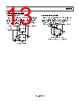
12 / 16 page  ADP3330 Data Sheet CALCULATING JUNCTION TEMPERATURE Device power dissipation is calculated as follows: PD = (VIN − VOUT) ILOAD + (VIN) IGND where: ILOAD and IGND are load current and ground current. VIN and VOUT are input and output voltages, respectively. Assuming ILOAD = 200 mA, IGND = 4 mA, VIN = 4.2 V, and VOUT = 3.0 V, the device power dissipation is the following: PD = (4.2 − 3.0) 200 mA + 4.2 (4 mA) = 257 mW The proprietary package used in the ADP3330 has a thermal resistance of 165°C/W, significantly lower than the standard 6-lead SOT-23 package. Assuming a 4-layer board, the junction temperature rise above ambient temperature is approximately equal to ΔTJA = 0.257 W × 165°C/W = 42.4°C To limit the maximum junction temperature to 125°C, maximum allowable ambient temperature is TA MAX = 125°C − 42.4°C = 82.6°C PRINTED CIRCUIT BOARD (PCB) LAYOUT CONSIDERATIONS All packages rely on the traces of the PCB to conduct heat away from the package. In standard packages, the dominant component of the heat resistance path is the plastic between the die attach pad and the individual leads. In typical thermally enhanced packages, one or more of the leads are fused to the die attach pad, significantly decreasing this component. To make the improvement meaningful, however, a significant copper area on the PCB must be attached to these fused pins. The patented chip-on-lead frame design of the ADP3330 uniformly minimizes the value of the dominant portion of the thermal resistance. It ensures that heat is conducted away by all of the package pins and yields a very low 165°C/W thermal resistance for the 6-lead SOT-23 package. Low thermal resistance is achieved without any special board layout requirements, just the normal traces connected to the leads, and yields a 17% improvement in heat dissipation capability as compared to a standard 6-lead SOT-23 package. The thermal resistance can be decreased by approximately an additional 10% by attaching a few square cm of copper area to the VIN pin of the ADP3330 package. It is not recommended to use solder mask or silkscreen on the PCB traces adjacent to the pins of the ADP3330 because it increases the junction to ambient thermal resistance of the package. ERROR FLAG DROPOUT DETECTOR The ADP3330 maintains its output voltage over a wide range of load, input voltage, and temperature conditions. If the output is about to lose regulation by reducing the supply voltage less than the combined regulated output and dropout voltages, the ERR flag is activated. The ERR output is an open collector that is driven low. When the ERR output is set, the hysteresis of the ERR flag keeps the output low until a small margin of the operating range is restored either by raising the supply voltage or reducing the load. SHUTDOWN MODE Applying a TTL high signal to the shutdown (SD) pin, or tying the SD pin to the input pin, turns the output on. Pulling the SD pin down to 0.4 V or below, or tying the SD pin to ground, turns the output off (we do not do all caps for emphasis). In shutdown mode, the ground current is reduced to much less than 1 µA. LOW POWER, LOW DROPOUT APPLICATIONS The ADP3330 is well suited for applications such as cell phone handsets that require low ground current and low dropout voltage features. The ADP3330 typically draws 34 µA under light load situations (that is, load current = 100 µA), which results in low power consumption when the cell phone is in standby mode. Figure 26 shows an application in which the ADP3330 is used in a handset to provide 2.75 V nominal output voltage. The cell phone is powered from a 3 cell NiCd or 1 cell Li-Ion battery. The ADP3330 guarantees an accuracy of 1.4%, even when the input/output differential is merely 250 mV (worst case). Therefore, the voltage output is regulated and within specification even when the battery voltage has reached its end of discharge voltage of 3 V. The output voltage never falls less than 2.7 V, even under worst case load and temperature conditions. The low dropout feature coupled with the high accuracy of the ADP3330 ensures that the system is reliably powered until the end of the life of the battery, which results in increased system talk time. Figure 26. LDO Budgeting for a 3 Cell NiCd/1 Cell Li-Ion Supply MINIMUM BATTERY VOLTAGE 3.0V NOMINAL OUTPUT VOLTAGE 2.75V 2.712V ABSOLUTE MINIMUM OUTPUT VOLTAGE 2.700V END OF DISCHARGE VOLTAGE OF 3 CELL NiCd OR 1 CELL Li-Ion BATTERY 250mV MAXIMUM INPUT-OUTPUT OVERHEAD FOR 200mA OUTPUT CURRENT –1.4% OUTPUT VOLTAGE ACCURACY 12mV TRANSIENT, LINE AND LOAD RESPECTIVE MARGIN Rev. C | Page 12 of 16 |
|
|
Enlace URL |
| ¿ALLDATASHEET es útil para Ud.? [ DONATE ] |
Todo acerca de Alldatasheet | Publicidad | Contáctenos | Política de Privacidad | Enlace a la hoja de datos | Intercambio de Enlaces | Lista de Fabricantes All Rights Reserved©Alldatasheet.com |
| Russian : Alldatasheetru.com | Korean : Alldatasheet.co.kr | Spanish : Alldatasheet.es | French : Alldatasheet.fr | Italian : Alldatasheetit.com Portuguese : Alldatasheetpt.com | Polish : Alldatasheet.pl | Vietnamese : Alldatasheet.vn Indian : Alldatasheet.in | Mexican : Alldatasheet.com.mx | British : Alldatasheet.co.uk | New Zealand : Alldatasheet.co.nz |
|
Family Site : ic2ic.com |
icmetro.com |
 Mexican ▼
 English
 Chinese
 German
 Japanese
 Russian
 Korean
 Spanish
 French
 Italian
 Portuguese
 Polish
 Vietnamese
 Indian
 Mexican
 British
 New Zealand