|
Motor de Búsqueda de Datasheet de Componentes Electrónicos |
|
|
Motor de Búsqueda de Datasheet de Componentes Electrónicos |
|
ADP3330ARTZ-2.5-R7 Datasheet(PDF) 2 Page - Analog Devices |
|
|
|||||||||||||||||||||||||||||
ADP3330ARTZ-2.5-R7 Datasheet(HTML) 2 Page - Analog Devices |
|
|
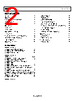
2 / 16 page  ADP3330 Data Sheet TABLE OF CONTENTS Features .............................................................................................. 1 Applications....................................................................................... 1 Simplified Functional Block Diagram ........................................... 1 General Description......................................................................... 1 Revision History ............................................................................... 2 Specifications..................................................................................... 3 ADP3330........................................................................................ 3 ADP3330-2.5................................................................................. 4 Absolute Maximum Ratings............................................................ 5 ESD Caution.................................................................................. 5 Pin Configuration and Function Descriptions............................. 6 Typical Performance Characteristics ............................................. 7 Theory of Operation ...................................................................... 10 Applications Information .............................................................. 11 Capacitor Selection .................................................................... 11 Noise Reduction ......................................................................... 11 Chip-on-Lead Package .............................................................. 11 Thermal Overload Protection .................................................. 11 Calculating Junction Temperature........................................... 12 Printed Circuit Board (PCB) Layout Considerations ........... 12 Error Flag Dropout Detector.................................................... 12 Shutdown Mode ......................................................................... 12 Low Power, Low Dropout Applications .................................. 12 Application Circuits ....................................................................... 13 Crossover Switch ........................................................................ 13 Higher Output Current ............................................................. 13 Outline Dimensions....................................................................... 14 Ordering Guide .......................................................................... 14 REVISION HISTORY 5/15—Rev. B to Rev. C Changes to General Description Section ...................................... 1 Changes to Chip-On-Lead Package Section............................... 11 Changes to Ordering Guide .......................................................... 14 5/14—Rev. A to Rev. B Updated Format..................................................................Universal Changed 0.47 mF to 0.47 µF, Features Section ............................. 1 Changes to General Description Section ...................................... 1 Changed −2.5 V to 2.5 V, ADP3330-xx Section .......................... 3 Changes to Table 1............................................................................ 3 Changes to Table 2............................................................................ 4 Changes to Figure 4 Caption through Figure 7 Caption............. 7 Changes to Figure 10, Figure 13 Caption, Figure 14 Caption, and Figure 15..................................................................................... 8 Changes to Figure 16, Figure 17, and Figure 19 Caption............ 9 Changes to Printed Circuit Board (PCB) Layout Considerations Section, and Low Power, Low Dropout Applications Section.. 12 Updated Outline Dimensions....................................................... 14 Changes to Ordering Guide .......................................................... 14 8/99—Rev. 0 to Rev. A Rev. C | Page 2 of 16 |
|
|
Enlace URL |
| ¿ALLDATASHEET es útil para Ud.? [ DONATE ] |
Todo acerca de Alldatasheet | Publicidad | Contáctenos | Política de Privacidad | Enlace a la hoja de datos | Intercambio de Enlaces | Lista de Fabricantes All Rights Reserved©Alldatasheet.com |
| Russian : Alldatasheetru.com | Korean : Alldatasheet.co.kr | Spanish : Alldatasheet.es | French : Alldatasheet.fr | Italian : Alldatasheetit.com Portuguese : Alldatasheetpt.com | Polish : Alldatasheet.pl | Vietnamese : Alldatasheet.vn Indian : Alldatasheet.in | Mexican : Alldatasheet.com.mx | British : Alldatasheet.co.uk | New Zealand : Alldatasheet.co.nz |
|
Family Site : ic2ic.com |
icmetro.com |
 Mexican ▼
 English
 Chinese
 German
 Japanese
 Russian
 Korean
 Spanish
 French
 Italian
 Portuguese
 Polish
 Vietnamese
 Indian
 Mexican
 British
 New Zealand