|
Motor de Búsqueda de Datasheet de Componentes Electrónicos |
|
|
Motor de Búsqueda de Datasheet de Componentes Electrónicos |
|
AN2647 Datasheet(PDF) 20 Page - STMicroelectronics |
|
|
|||||||||||||||||||||||||||||
AN2647 Datasheet(HTML) 20 Page - STMicroelectronics |
|
|
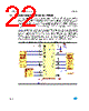
20 / 34 page  Interfacing with synchronous memory AN2647 20/34 2.1 PSRAM overview The key functional block of the MT45W4M (MT45W4MW16BC), as shown in Figure 10 on page 21, consists of a 4096K x 16 DRAM memory array, the Control Logic, the Configuration registers and the Input/Output Buffer. The Bus Configuration Register (BCR) controls the operating modes and timings of the MT45W4M. 2.1.1 Bus interface signals The MT45W4M is usually connected to a non-multiplexed bus, with a 16-bit data bus and 23 address inputs. However, it can be configured to interface to a multiplexed bus like the STR91xFA EMI bus. In addition to the standard SRAM control signals such as CE, OE, WE, UB and LB, the PSRAM has four additional signals that are required for synchronous (burst) mode operation and are described in Table 7. Table 7. PSRAM control signals Signal name Type Description CLK Input Clock: Synchronizes the memory to the system operating frequency during synchronous operations. When configured for synchronous operation, the address is latched on the first rising CLK edge when ADV# is active. CLK must be static LOW during asynchronous access READ and WRITE operations ADV# Input Address valid: Indicates that a valid address is present on the address inputs. Addresses can be latched on the rising edge of ADV# during asynchronous READ and WRITE operations. CRE Input Control register enable: When CRE is HIGH, WRITE operations load the RCR or BCR registers, and READ operations access the RCR, BCR, or DIDR registers. Wait Output Wait: Provides data-valid feedback during burst READ and WRITE operations. WAIT is used to arbitrate collisions between refresh and READ/WRITE operations. WAIT is asserted at the end of a row. WAIT is asserted and should be ignored during asynchronous mode. CE# Input Chip enable: Activates the device when LOW. When CE# is HIGH, the device is disabled and goes into standby or deep power-down mode. OE# Input Output enable: Enables the output buffers when LOW. When OE# is HIGH, the output buffers are disabled. WE# Input Write enable: Determines if a given cycle is a WRITE cycle. If WE# is LOW, the cycle is a WRITE to either a configuration register or to the memory array. LB# Input Lower byte enable. DQ[7:0] UB# Input Upper byte enable. DQ[15:8] |
|
Enlace URL |
| ¿ALLDATASHEET es útil para Ud.? [ DONATE ] |
Todo acerca de Alldatasheet | Publicidad | Contáctenos | Política de Privacidad | Enlace a la hoja de datos | Intercambio de Enlaces | Lista de Fabricantes All Rights Reserved©Alldatasheet.com |
| Russian : Alldatasheetru.com | Korean : Alldatasheet.co.kr | Spanish : Alldatasheet.es | French : Alldatasheet.fr | Italian : Alldatasheetit.com Portuguese : Alldatasheetpt.com | Polish : Alldatasheet.pl | Vietnamese : Alldatasheet.vn Indian : Alldatasheet.in | Mexican : Alldatasheet.com.mx | British : Alldatasheet.co.uk | New Zealand : Alldatasheet.co.nz |
|
Family Site : ic2ic.com |
icmetro.com |
 Mexican ▼
 English
 Chinese
 German
 Japanese
 Russian
 Korean
 Spanish
 French
 Italian
 Portuguese
 Polish
 Vietnamese
 Indian
 Mexican
 British
 New Zealand