|
Motor de Búsqueda de Datasheet de Componentes Electrónicos |
|
|
Motor de Búsqueda de Datasheet de Componentes Electrónicos |
|
ADE7758 Datasheet(PDF) 38 Page - Analog Devices |
|
|
|||||||||||||||||||||||||||||
ADE7758 Datasheet(HTML) 38 Page - Analog Devices |
|
|
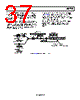
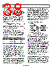
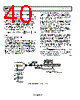
38 / 72 page  ADE7758 Data Sheet Rev. E | Page 38 of 72 Integration Time Under Steady Load The discrete time sample period (T) for the accumulation register is 0.4 μs (4/CLKIN). With full-scale sinusoidal signals on the analog inputs, a 90° phase difference between the voltage and the current signal (the largest possible reactive power), and the VAR gain registers set to 0x000, the average word value from each LPF2 is 0xCCCCD. The maximum value that can be stored in the reactive energy register before it overflows is 215 − 1 or 0x7FFF. Because the average word value is added to the internal register, which can store 240 − 1 or 0xFF, FFFF, FFFF before it overflows, the integration time under these conditions with VARDIV = 0 is calculated as sec 0.5243 μs 0.4 0xCCCCD FFFF FFFF, 0xFF, = × = Time (36) When VARDIV is set to a value different from 0, the time before overflow are scaled accordingly as shown in Equation 37. Time = Time(VARDIV = 0) × VARDIV (37) Energy Accumulation Mode The reactive power accumulated in each VAR-hr accumulation register (AVARHR, BVARHR, or CVARHR) depends on the configuration of the CONSEL bits in the COMPMODE register (Bit 0 and Bit 1). The different configurations are described in Table 13. Note that IA’/IB’/IC’ are the current phase-shifted current waveform. Table 13. Inputs to VAR-Hr Accumulation Registers CONSEL[1, 0] AVARHR BVARHR CVARHR 00 VA × IA’ VB × IB VC × IC’ 01 VA (IA’ – IB’) 0 VC (IC’ – IB’) 10 VA (IA’ – IB’) 0 VC × IC’ 11 Reserved Reserved Reserved Reactive Power Frequency Output Pin 17 (VARCF) of the ADE7758 provides frequency output for the total reactive power. Similar to APCF, this pin provides an output frequency that is directly proportional to the total reactive power. The pulse width of VARPCF is 64/CLKIN if VARCFNUM and VARCFDEN are both equal. If VARCFDEN is greater than VARCFNUM, the pulse width depends on VARCFDEN. The pulse width in this case is T × (VARCFDEN/2), where T is the period of the VARCF pulse and VARCFDEN/2 is rounded to the nearest whole number. An exception to this is when the period is greater than 180 ms. In this case, the pulse width is fixed at 90 ms. A digital-to-frequency converter (DFC) is used to generate the VARCF pulse output from the total reactive power. The TERMSEL bits (Bit 2 to Bit 4) of the COMPMODE register can be used to select which phases to include in the total reactive power calcu- lation. Setting Bit 2, Bit 3, and Bit 4 includes the input to the AVARHR, BVARHR, and CVARHR registers in the total reactive power calculation. The total reactive power is signed addition. However, setting the SAVAR bit (Bit 6) in the COMPMODE register enables absolute value calculation. If the active power of that phase is positive, no change is made to the sign of the reactive power. However, if the sign of the active power is negative in that phase, the sign of its reactive power is inverted before summing and creating VARCF pulses. This mode should be used in conjunction with the absolute value mode for active power (Bit 5 in the COMPMODE register) for APCF pulses. The effects of setting the ABS and SAVAR bits of the COMPMODE register are as follows when ABS = 1 and SAVAR = 1: If watt > 0, APCF = Watts, VARCF = +VAR. If watt < 0, APCF = |Watts|, VARCF = −VAR. INPUT TO BVARHR REGISTER INPUT TO AVARHR REGISTER INPUT TO CVARHR REGISTER + + + INPUT TO BVAHR REGISTER INPUT TO AVAHR REGISTER INPUT TO CVAHR REGISTER + + + 0 1 VARCF VARCFNUM[11:0] VARCFDEN[11:0] ÷ DFC VACF BIT (BIT 7) OF WAVMODE REGISTER ÷4 Figure 74. Reactive Power Frequency Output The output from the DFC is divided down by a pair of frequency division registers before sending to the VARCF pulse output. Namely, VARCFDEN/VARCFNUM pulses are needed at the DFC output before the VARCF pin outputs a pulse. Under steady load conditions, the output frequency is directly proportional to the total reactive power. Figure 74 illustrates the energy-to-frequency conversion in the ADE7758. Note that the input to the DFC can be selected between the total reactive power and total apparent power. Therefore, the VARCF pin can output frequency that is proportional to the total reactive power or total apparent power. The selection is made by setting the VACF bit (Bit 7) in the WAVMODE register. Setting this bit switches the input to the total apparent power. The default value of this bit is logic low. Therefore, the default output from the VARCF pin is the total reactive power. All other operations of this frequency output are similar to that of the active power frequency output (see the Active Power Frequency Output section). Line Cycle Reactive Energy Accumulation Mode The line cycle reactive energy accumulation mode is activated by setting the LVAR bit (Bit 1) in the LCYCMODE register. The total reactive energy accumulated over an integer number of zero crossings is written to the VAR-hr accumulation registers after the LINECYC number of zero crossings is detected. The operation of this mode is similar to watt-hr accumulation (see the Line Cycle Active Energy Accumulation Mode section). |
|
Enlace URL |
| ¿ALLDATASHEET es útil para Ud.? [ DONATE ] |
Todo acerca de Alldatasheet | Publicidad | Contáctenos | Política de Privacidad | Enlace a la hoja de datos | Intercambio de Enlaces | Lista de Fabricantes All Rights Reserved©Alldatasheet.com |
| Russian : Alldatasheetru.com | Korean : Alldatasheet.co.kr | Spanish : Alldatasheet.es | French : Alldatasheet.fr | Italian : Alldatasheetit.com Portuguese : Alldatasheetpt.com | Polish : Alldatasheet.pl | Vietnamese : Alldatasheet.vn Indian : Alldatasheet.in | Mexican : Alldatasheet.com.mx | British : Alldatasheet.co.uk | New Zealand : Alldatasheet.co.nz |
|
Family Site : ic2ic.com |
icmetro.com |
 Mexican ▼
 English
 Chinese
 German
 Japanese
 Russian
 Korean
 Spanish
 French
 Italian
 Portuguese
 Polish
 Vietnamese
 Indian
 Mexican
 British
 New Zealand