|
Motor de Búsqueda de Datasheet de Componentes Electrónicos |
|
|
Motor de Búsqueda de Datasheet de Componentes Electrónicos |
|
ADE7758 Datasheet(PDF) 57 Page - Analog Devices |
|
|
|||||||||||||||||||||||||||||
ADE7758 Datasheet(HTML) 57 Page - Analog Devices |
|
|
57 / 72 page 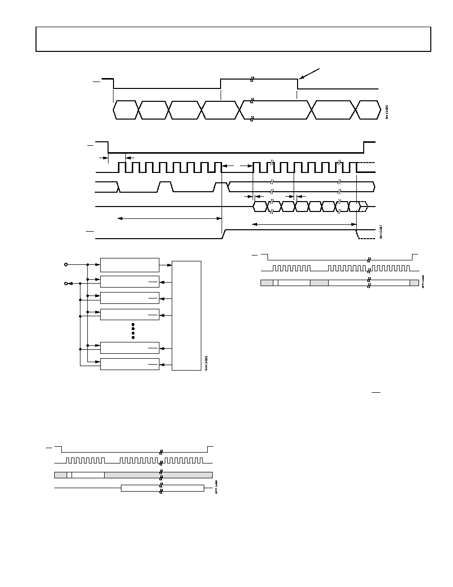 Data Sheet ADE7758 Rev. E | Page 57 of 72 GLOBAL INTERRUPT MASK ISR RETURN GLOBAL INTERRUPT MASK RESET CLEAR MCU INTERRUPT FLAG READ STATUS WITH RESET (0x1A) ISR ACTION (BASED ON STATUS CONTENTS) MCU INTERRUPT FLAG SET PROGRAM SEQUENCE t1 t2 t3 JUMP TO ISR JUMP TO ISR IRQ Figure 87. ADE7758 Interrupt Management STATUS REGISTER CONTENTS SCLK DIN DOUT READ STATUS REGISTER COMMAND t1 CS 00 0 1 00 0 DB15 DB8 DB7 DB0 1 t9 t11 t12 IRQ Figure 88. ADE7758 Interrupt Timing COMMUNICATIONS REGISTER IN OUT IN OUT IN OUT IN OUT IN OUT REGISTER NO. 1 REGISTER NO. 2 REGISTER NO. 3 REGISTER NO. n–1 REGISTER NO. n REGISTER ADDRESS DECODE DIN DOUT Figure 89. Addressing ADE7758 Registers via the Communications Register The communications register is an 8-bit, write-only register. The MSB determines whether the next data transfer operation is a read or a write. The seven LSBs contain the address of the register to be accessed (see Table 16). Figure 90 and Figure 91 show the data transfer sequences for a read and write operation, respectively. MULTIBYTE COMMUNICATIONS REGISTER WRITE DIN SCLK DOUT READ DATA ADDRESS 0 CS Figure 90. Reading Data from the ADE7758 via the Serial Interface COMMUNICATIONS REGISTER WRITE DIN SCLK ADDRESS 1 CS MULTIBYTE READ DATA Figure 91. Writing Data to the ADE7758 via the Serial Interface On completion of a data transfer (read or write), the ADE7758 once again enters into communications mode, that is, the next instruction followed must be a write to the communications register. A data transfer is completed when the LSB of the ADE7758 register being addressed (for a write or a read) is transferred to or from the ADE7758. SERIAL WRITE OPERATION The serial write sequence takes place as follows. With the ADE7758 in communications mode and the CS input logic low, a write to the communications register takes place first. The MSB of this byte transfer must be set to 1, indicating that the next data transfer operation is a write to the register. The seven LSBs of this byte contain the address of the register to be written to. The starts shifting in the register data on the next falling edge of SCLK. All remaining bits of register data are shifted in on the falling edge of the subsequent SCLK pulses (see ). ADE7758 Figure 92 |
|
Enlace URL |
| ¿ALLDATASHEET es útil para Ud.? [ DONATE ] |
Todo acerca de Alldatasheet | Publicidad | Contáctenos | Política de Privacidad | Enlace a la hoja de datos | Intercambio de Enlaces | Lista de Fabricantes All Rights Reserved©Alldatasheet.com |
| Russian : Alldatasheetru.com | Korean : Alldatasheet.co.kr | Spanish : Alldatasheet.es | French : Alldatasheet.fr | Italian : Alldatasheetit.com Portuguese : Alldatasheetpt.com | Polish : Alldatasheet.pl | Vietnamese : Alldatasheet.vn Indian : Alldatasheet.in | Mexican : Alldatasheet.com.mx | British : Alldatasheet.co.uk | New Zealand : Alldatasheet.co.nz |
|
Family Site : ic2ic.com |
icmetro.com |
 Mexican ▼
 English
 Chinese
 German
 Japanese
 Russian
 Korean
 Spanish
 French
 Italian
 Portuguese
 Polish
 Vietnamese
 Indian
 Mexican
 British
 New Zealand