|
Motor de Búsqueda de Datasheet de Componentes Electrónicos |
|
|
Motor de Búsqueda de Datasheet de Componentes Electrónicos |
|
ADE7758 Datasheet(PDF) 61 Page - Analog Devices |
|
|
|||||||||||||||||||||||||||||
ADE7758 Datasheet(HTML) 61 Page - Analog Devices |
|
|
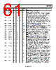
61 / 72 page  Data Sheet ADE7758 Rev. E | Page 61 of 72 Address [A6:A0] Name R/W1 Length Type2 Default Value Description 0x0E BVRMS R 24 S 0 Phase B Voltage Channel RMS Register. 0x0F CVRMS R 24 S 0 Phase C Voltage Channel RMS Register. 0x10 FREQ R 12 U 0 Frequency of the Line Input Estimated by the Zero-Crossing Processing. It can also display the period of the line input. Bit 7 of the LCYCMODE register determines if the reading is frequency or period. Default is frequency. Data Bit 0 and Bit 1 of the MMODE register determine the voltage channel used for the frequency or period calculation. 0x11 TEMP R 8 S 0 Temperature Register. This register contains the result of the latest temperature conversion. Refer to the Temperature Measurement section for details on how to interpret the content of this register. 0x12 WFORM R 24 S 0 Waveform Register. This register contains the digitized waveform of one of the six analog inputs or the digitized power waveform. The source is selected by Data Bit 0 to Bit 4 in the WAVMODE register. 0x13 OPMODE R/W 8 U 4 Operational Mode Register. This register defines the general configuration of the ADE7758 (see Table 18). 0x14 MMODE R/W 8 U 0xFC Measurement Mode Register. This register defines the channel used for period and peak detection measurements (see Table 19). 0x15 WAVMODE R/W 8 U 0 Waveform Mode Register. This register defines the channel and sampling frequency used in the waveform sampling mode (see Table 20). 0x16 COMPMODE R/W 8 U 0x1C Computation Mode Register. This register configures the formula applied for the energy and line active energy measurements (see Table 22). 0x17 LCYCMODE R/W 8 U 0x78 Line Cycle Mode Register. This register configures the line cycle accumulation mode for WATT-HR, VAR-HR, and VA-Hr (see Table 23). 0x18 Mask R/W 24 U 0 IRQ Mask Register. It determines if an interrupt event generates an active-low output at the IRQ pin (see the section). Interrupts 0x19 Status R 24 U 0 IRQ Status Register. This register contains information regarding the source of the interrupts (see the section). ADE7758 Interrupts 0x1A RSTATUS R 24 U 0 IRQ Reset Status Register. Same as the STATUS register, except that its contents are reset to 0 (all flags cleared) after a read operation. 0x1B ZXTOUT R/W 16 U 0xFFFF Zero-Cross Timeout Register. If no zero crossing is detected within the time period specified by this register, the interrupt request line (IRQ) goes active low for the corresponding line voltage. The maximum timeout period is 2.3 seconds (see the section). Zero-Crossing Detection 0x1C LINECYC R/W 16 U 0xFFFF Line Cycle Register. The content of this register sets the number of half-line cycles that the active, reactive, and apparent energies are accumulated for in the line accumulation mode. 0x1D SAGCYC R/W 8 U 0xFF SAG Line Cycle Register. This register specifies the number of consecutive half-line cycles where voltage channel input may fall below a threshold level. This register is common to the three line voltage SAG detection. The detection threshold is specified by the SAGLVL register (see the Line Voltage SAG Detection section). 0x1E SAGLVL R/W 8 U 0 SAG Voltage Level. This register specifies the detection threshold for the SAG event. This register is common to all three phases’ line voltage SAG detections. See the description of the SAGCYC register for details. 0x1F VPINTLVL R/W 8 U 0xFF Voltage Peak Level Interrupt Threshold Register. This register sets the level of the voltage peak detection. Bit 5 to Bit 7 of the MMODE register determine which phases are to be monitored. If the selected voltage phase exceeds this level, the PKV flag in the IRQ status register is set. 0x20 IPINTLVL R/W 8 U 0xFF Current Peak Level Interrupt Threshold Register. This register sets the level of the current peak detection. Bit 5 to Bit 7 of the MMODE register determine which phases are to be monitored. If the selected current phase exceeds this level, the PKI flag in the IRQ status register is set. 0x21 VPEAK R 8 U 0 Voltage Peak Register. This register contains the value of the peak voltage waveform that has occurred within a fixed number of half-line cycles. The number of half-line cycles is set by the LINECYC register. |
|
Enlace URL |
| ¿ALLDATASHEET es útil para Ud.? [ DONATE ] |
Todo acerca de Alldatasheet | Publicidad | Contáctenos | Política de Privacidad | Enlace a la hoja de datos | Intercambio de Enlaces | Lista de Fabricantes All Rights Reserved©Alldatasheet.com |
| Russian : Alldatasheetru.com | Korean : Alldatasheet.co.kr | Spanish : Alldatasheet.es | French : Alldatasheet.fr | Italian : Alldatasheetit.com Portuguese : Alldatasheetpt.com | Polish : Alldatasheet.pl | Vietnamese : Alldatasheet.vn Indian : Alldatasheet.in | Mexican : Alldatasheet.com.mx | British : Alldatasheet.co.uk | New Zealand : Alldatasheet.co.nz |
|
Family Site : ic2ic.com |
icmetro.com |
 Mexican ▼
 English
 Chinese
 German
 Japanese
 Russian
 Korean
 Spanish
 French
 Italian
 Portuguese
 Polish
 Vietnamese
 Indian
 Mexican
 British
 New Zealand