|
Motor de Búsqueda de Datasheet de Componentes Electrónicos |
|
|
Motor de Búsqueda de Datasheet de Componentes Electrónicos |
|
ADE7758 Datasheet(PDF) 58 Page - Analog Devices |
|
|
|||||||||||||||||||||||||||||
ADE7758 Datasheet(HTML) 58 Page - Analog Devices |
|
|
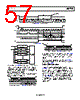
58 / 72 page  ADE7758 Data Sheet Rev. E | Page 58 of 72 As explained earlier, the data write is initiated by a write to the communications register followed by the data. During a data write operation to the ADE7758, data is transferred to all on- chip registers one byte at a time. After a byte is transferred into the serial port, there is a finite time duration before the content in the serial port buffer is transferred to one of the ADE7758 on-chip registers. Although another byte transfer to the serial port can start while the previous byte is being transferred to the destination register, this second-byte transfer should not finish until at least 900 ns after the end of the previous byte transfer. This functionality is expressed in the timing specification t6 (see Figure 92). If a write operation is aborted during a byte transfer (CS brought high), then that byte is not written to the destination register. Destination registers can be up to 3 bytes wide (see the Accessing the On-Chip Registers section). Therefore, the first byte shifted into the serial port at DIN is transferred to the most significant byte (MSB) of the destination register. If the destination register is 12 bits wide, for example, a two-byte data transfer must take place. The data is always assumed to be right justified; therefore, in this case, the four MSBs of the first byte would be ignored, and the four LSBs of the first byte written to the ADE7758 would be the four MSBs of the 12-bit word. Figure 93 illustrates this example. DIN SCLK CS t2 t3 t1 t4 t5 t7 t6 t8 COMMAND BYTE MOST SIGNIFICANT BYTE LEAST SIGNIFICANT BYTE 1A6 A4 A5 A3 A2 A1 A0 DB7 DB0 DB7 DB0 t7 Figure 92. Serial Interface Write Timing Diagram SCLK DIN X X X X DB11 DB10 DB9 DB8 DB7 DB6 DB5 DB4 DB3 DB2 DB1 DB0 MOST SIGNIFICANT BYTE LEAST SIGNIFICANT BYTE Figure 93. 12-Bit Serial Write Operation SCLK CS t1 t10 t13 0 A6 A4 A5 A3 A2 A1 A0 DB0 DB7 DB0 DB7 DIN DOUT t11 t12 COMMAND BYTE MOST SIGNIFICANT BYTE LEAST SIGNIFICANT BYTE t9 Figure 94. Serial Interface Read Timing Diagram |
|
Enlace URL |
| ¿ALLDATASHEET es útil para Ud.? [ DONATE ] |
Todo acerca de Alldatasheet | Publicidad | Contáctenos | Política de Privacidad | Enlace a la hoja de datos | Intercambio de Enlaces | Lista de Fabricantes All Rights Reserved©Alldatasheet.com |
| Russian : Alldatasheetru.com | Korean : Alldatasheet.co.kr | Spanish : Alldatasheet.es | French : Alldatasheet.fr | Italian : Alldatasheetit.com Portuguese : Alldatasheetpt.com | Polish : Alldatasheet.pl | Vietnamese : Alldatasheet.vn Indian : Alldatasheet.in | Mexican : Alldatasheet.com.mx | British : Alldatasheet.co.uk | New Zealand : Alldatasheet.co.nz |
|
Family Site : ic2ic.com |
icmetro.com |
 Mexican ▼
 English
 Chinese
 German
 Japanese
 Russian
 Korean
 Spanish
 French
 Italian
 Portuguese
 Polish
 Vietnamese
 Indian
 Mexican
 British
 New Zealand