|
Motor de Búsqueda de Datasheet de Componentes Electrónicos |
|
|
Motor de Búsqueda de Datasheet de Componentes Electrónicos |
|
ADE7758 Datasheet(PDF) 27 Page - Analog Devices |
|
|
|||||||||||||||||||||||||||||
ADE7758 Datasheet(HTML) 27 Page - Analog Devices |
|
|
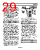
27 / 72 page  Data Sheet ADE7758 Rev. E | Page 27 of 72 On the ADE7758, if the regular succession of the zero crossings presented above happens, the SEQERR bit (Bit 19) in the STATUS register is set (Figure 60). If SEQERR is set in the mask register, the IRQ logic output goes active low (see the section). Interrupts If the regular zero crossing succession does not occur, that is when a negative to positive transition on Phase A followed by a positive to negative transition on Phase B, followed by a negative to positive transition on Phase C, and so on, the SEQERR bit (Bit 19) in the STATUS register is cleared to 0. To have the ADE7758 trigger SEQERR status bit when the zero crossing regular succession does not occur, the analog inputs for Phase C and Phase B should be swapped. In this case, the Phase B voltage input should be wired to the VCP pin, and the Phase C voltage input should be wired to the VBP pin. AB SEQERR BIT OF STATUS REGISTER IS SET A = 0° B = –120° C = +120° C VOLTAGE WAVEFORMS ZERO CROSSINGS C A B C A C A B Figure 60. Regular Phase Sequence Sets SEQERR Bit to 1 AC SEQERR BIT OF STATUS REGISTER IS NOT SET A = 0° C = –120° B = +120° B ZERO CROSSINGS VOLTAGE WAVEFORMS B A C B A B A C Figure 61. Erroneous Phase Sequence Clears SEQERR Bit to 0 POWER-SUPPLY MONITOR The ADE7758 also contains an on-chip power-supply monitor. The analog supply (AVDD) is monitored continuously by the ADE7758. If the supply is less than 4 V ± 5%, the ADE7758 goes into an inactive state, that is, no energy is accumulated when the supply voltage is below 4 V. This is useful to ensure correct device operation at power-up and during power-down. The power-supply monitor has built-in hysteresis and filtering. This gives a high degree of immunity to false triggering due to noisy supplies. When AVDD returns above 4 V ± 5%, the ADE7758 waits 18 μs for the voltage to achieve the recommended voltage range, 5 V ± 5% and then becomes ready to function. Figure 62 shows the behavior of the ADE7758 when the voltage of AVDD falls below the power-supply monitor threshold. The power supply and decoupling for the part should be designed such that the ripple at AVDD does not exceed 5 V ± 5% as specified for normal operation. AVDD 5V 4V 0V ADE7758 INTERNAL CALCULATIONS ACTIVE INACTIVE INACTIVE TIME Figure 62. On-Chip, Power-Supply Monitoring REFERENCE CIRCUIT The nominal reference voltage at the REFIN/OUT pin is 2.42 V. This is the reference voltage used for the ADCs in the ADE7758. However, the current channels have three input range selections (full scale is selectable among 0.5 V, 0.25 V, and 0.125 V). This is achieved by dividing the reference internally by 1, ½, and ¼. The reference value is used for the ADC in the current channels. Note that the full-scale selection is only available for the current inputs. The REFIN/OUT pin can be overdriven by an external source, for example, an external 2.5 V reference. Note that the nominal reference value supplied to the ADC is now 2.5 V and not 2.42 V. This has the effect of increasing the nominal analog input signal range by 2.5/2.42 × 100% = 3% or from 0.5 V to 0.5165 V. The voltage of the ADE7758 reference drifts slightly with temperature; see the Specifications section for the temperature coefficient specification (in ppm/°C). The value of the temperature drift varies from part to part. Because the reference is used for all ADCs, any ×% drift in the reference results in a 2×% deviation of the meter accuracy. The reference drift resulting from temperature changes is usually very small and typically much smaller than the drift of other components on a meter. Alternatively, the meter can be calibrated at multiple temperatures. TEMPERATURE MEASUREMENT The ADE7758 also includes an on-chip temperature sensor. A temperature measurement is made every 4/CLKIN seconds. The output from the temperature sensing circuit is connected to an ADC for digitizing. The resultant code is processed and placed in the temperature register (TEMP[7:0]). This register can be read by the user and has an address of 0x11 (see the Serial Interface section). The contents of the temperature register are signed (twos complement) with a resolution of 3°C/LSB. The offset of this register may vary significantly from part to part. To calibrate this register, the nominal value should be measured, and the equation should be adjusted accordingly. |
|
Enlace URL |
| ¿ALLDATASHEET es útil para Ud.? [ DONATE ] |
Todo acerca de Alldatasheet | Publicidad | Contáctenos | Política de Privacidad | Enlace a la hoja de datos | Intercambio de Enlaces | Lista de Fabricantes All Rights Reserved©Alldatasheet.com |
| Russian : Alldatasheetru.com | Korean : Alldatasheet.co.kr | Spanish : Alldatasheet.es | French : Alldatasheet.fr | Italian : Alldatasheetit.com Portuguese : Alldatasheetpt.com | Polish : Alldatasheet.pl | Vietnamese : Alldatasheet.vn Indian : Alldatasheet.in | Mexican : Alldatasheet.com.mx | British : Alldatasheet.co.uk | New Zealand : Alldatasheet.co.nz |
|
Family Site : ic2ic.com |
icmetro.com |
 Mexican ▼
 English
 Chinese
 German
 Japanese
 Russian
 Korean
 Spanish
 French
 Italian
 Portuguese
 Polish
 Vietnamese
 Indian
 Mexican
 British
 New Zealand